What is LDO: Theory, Parameters, and Practical Implementation for Engineers
This article explains what is LDO, how the LDO regulator works, discusses key specifications such as dropout voltage, line/load regulation, noise, and PSRR, and shows how to select and design with LDOs to meet demanding engineering requirements.

16 Feb, 2026. 15 minutes read
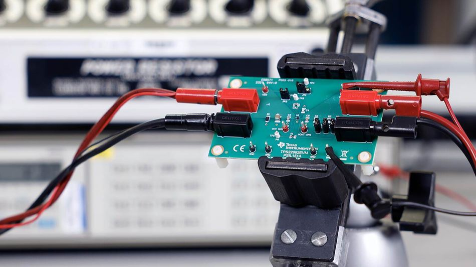
Low Dropout Regulator (LDO)
Key Takeaways
Understand LDO Fundamentals: A low‑dropout regulator is a type of linear regulator that maintains a stable output voltage even as the input approaches the output. LDOs are defined by their dropout voltage (<1 V), which allows them to operate with small input–output differentials.
Know the Critical Parameters: Parameters such as line regulation, load regulation, quiescent current, dropout voltage, power‑supply rejection ratio (PSRR) and output noise determine LDO performance. High PSRR and low noise are crucial for noise‑sensitive analog or RF circuits.
Use Appropriate Capacitors: Input (CIN), bias (CBIAS) and output (COUT) capacitors filter noise and ensure stability. Ceramic MLCC capacitors with low equivalent series resistance/inductance (ESR/ESL) are recommended, but their capacitance changes with voltage and temperature. Proper placement and selection of low‑ESL/ESR capacitors improve transient response and PSRR.
Evaluate Efficiency and Thermal Performance: LDO efficiency equals the ratio of output to input voltage when quiescent current is negligible. Designers must calculate power dissipation and junction temperature to ensure reliable operation.
Select the Right Device: Choose an LDO based on input and output voltage range, output current, dropout voltage, PSRR, noise, and protection features. For example, the TI LP5922 provides 2 A output current, 200 mV dropout at full load and 70 dB PSRR at 1 kHz, while the Toshiba TCR15AG series offers PSRR of around 95 dB.
Introduction
In modern electronic systems, efficient and stable voltage regulation is fundamental to performance, reliability, and noise control. When engineers evaluate linear-regulation solutions, a common question arises: what is LDO, and how does it differ from conventional linear or switching regulators?
The Low Dropout Regulator (LDO) is a linear voltage regulator designed to operate with a very small input-to-output voltage differential, enabling regulation even when the supply voltage is only slightly higher than the desired output. Understanding what is LDO is essential for designing power architectures in battery-powered devices, embedded systems, RF modules, and precision analog circuits.
From a theoretical standpoint, what is LDO involves examining pass elements, error amplifiers, reference voltages, and feedback loops that maintain output stability under varying load conditions. In practical engineering design, knowing what is LDO also requires evaluating parameters such as dropout voltage, quiescent current, power dissipation, PSRR, transient response, and thermal performance to ensure optimal implementation.
Fundamentals of LDO Regulators
How Linear Regulators Work?
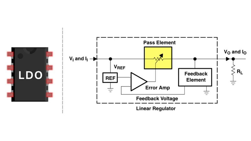
Linear regulators maintain a constant output by dropping the excess voltage from the input across an active device (pass transistor) operating in its linear region. In LDO regulators, this pass device is typically a MOSFET or bipolar transistor, controlled by an internal error amplifier and feedback loop.
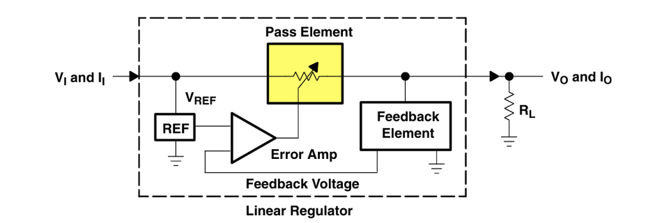
The basic block diagram consists of a pass device placed between the input voltage (VIN) and the regulated output, a precision reference voltage (often derived from a bandgap circuit), and a resistor divider network formed by external or internal resistors. The error amplifier compares the scaled VOUT to the reference and adjusts the pass-transistor gate voltage to correct deviations.
Because the pass device behaves as a variable resistance, excess energy from the power supply is dissipated as heat. Unlike switching regulators or a DC-DC converter, LDOs do not rely on high frequencies or energy storage components, such as inductors. This makes them inherently low-noise and suitable for sensitive analog and mixed-signal electronic devices.
Definition of Dropout Voltage
The defining parameter of a low dropout regulator is its dropout voltage (VDO) — the minimum voltage differential between input and output required to maintain regulation. Once the input voltage approaches VOUT, the pass device can no longer remain in its linear region, and regulation is lost.
For a MOSFET-based pass element, the dropout voltage is approximately:

where a smaller RDS(on) yields a lower dropout at a given output current. LDOs generally have VDO values under 1 V; devices requiring less than 1 V input–output differential are called low‑dropout regulators.
P‑Channel vs. N‑Channel Pass Devices
LDO architecture depends heavily on the selected semiconductor pass device.
Single-Supply LDOs commonly use a P-channel MOSFET. The gate is driven relative to VIN, simplifying design since only one supply voltage is required. However, as VIN approaches VOUT, the available gate drive reduces, increasing dropout voltage and limiting performance.
Dual-Supply LDOs use an N-channel MOSFET driven from an independent bias source. Because the gate voltage is no longer constrained by VIN, the device can achieve lower RDS(on), improved efficiency at high current, and better performance under low VIN conditions. This configuration is common in high-performance power management designs.
Line Regulation and Load Regulation
Two metrics quantify how well an LDO maintains VOUT when VIN or load current changes.
Line Regulation measures the change in output voltage with respect to changes in input voltage while keeping the load current constant. It is calculated as ΔVOUT/ΔVIN and is typically expressed in millivolts. Devices with small line regulation maintain a consistent output despite input variations.
Load Regulation quantifies the change in output voltage as the load current varies with a fixed input voltage. It is given by ΔVOUT/ΔIOUT. A low load regulation value indicates that the regulator maintains its output voltage across a wide range of load currents, which is important for digital systems that draw dynamic currents.
Together, these metrics reflect the effectiveness of the internal feedback loop, the strength of the pass element, and the stability of the control architecture.
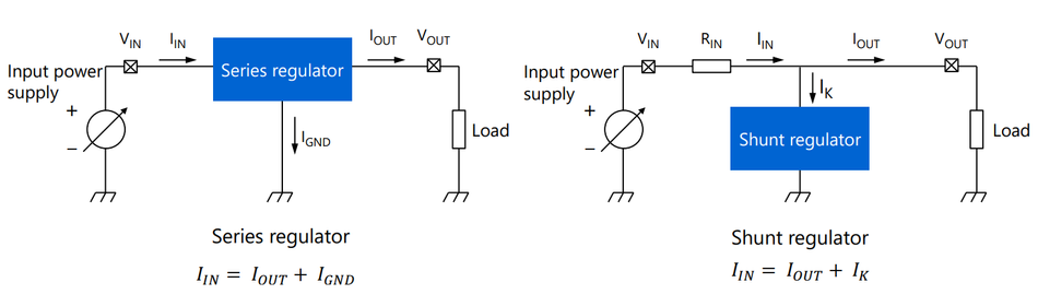
Linear Regulation vs. Switching Regulators
Because LDOs operate in a linear mode, the difference between VIN and VOUT results in power loss:

This affects power consumption and thermal performance, particularly at large voltage drops.
In contrast, switching regulators use energy storage elements and high-frequency switching to improve efficiency, especially for step-down conversion and high load currents. However, switching topologies introduces ripple, switching noise, and electromagnetic interference.
Engineers often combine a buck converter (DC-DC converter) with an LDO stage: the switching regulator provides efficient voltage conversion, while the LDO ensures high PSRR (power supply rejection ratio), reduced output noise, and clean regulation for sensitive analog or RF circuitry.
Recommended Reading: How Switching Regulators Work: Deep Dive for Power Engineers
Key Parameters and Performance Metrics
Input and Output Voltage Range
Every LDO has a specified VIN operating range and recommended output voltage range. For example, the Texas Instruments LP5922 supports a wide VIN range from 1.3 V to 6 V, adjustable output voltages from 0.5 V to 5 V, and provides 2 A of output current. [1] When selecting an LDO, ensure that the minimum input voltage exceeds the desired output voltage by at least the dropout voltage under all conditions.
Quiescent Current and Efficiency
Quiescent current (IQ) represents the internal bias current consumed by the control circuitry, including the error amplifier, bandgap reference, and bias networks. In CMOS-based LDO regulators, IQ can be extremely low, making them suitable for low-power battery-operated electronic devices and standby applications with shutdown functionality.
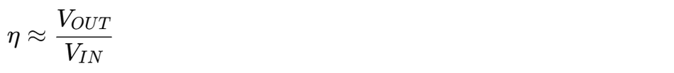
The efficiency of an LDO is defined as the ratio of output power to input power:
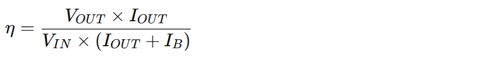
when output current is much larger than the quiescent current, efficiency approximates:
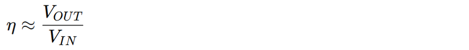
This highlights a fundamental limitation of linear voltage regulators: efficiency depends directly on the output-to-input voltage ratio. The large voltage drop increases power loss and overall power consumption, making LDOs less suitable than switching regulators or DC-DC converters for high step-down ratios or high-current applications.
Output Voltage Accuracy
Output accuracy defines how closely VOUT matches its nominal value across temperature, input variation, and load. High-precision devices maintain tight tolerances through stable reference voltage generation and well-designed feedback loops.
The accurate regulation prevents logic errors in microcontroller systems and maintains signal integrity in analog circuitry. Variations in resistors, temperature drift, and semiconductor mismatch within the pass element affect regulation accuracy, so designers must review guaranteed specifications rather than typical values.
Output Noise Voltage
Output noise (VNO) measures the intrinsic noise generated by the regulator. It is defined as the root‑mean‑square (RMS) sum of all noise within a specified bandwidth. The noise sources include:
1/f (Flicker) Noise: Dominant at low frequencies and caused by surface defects in semiconductors.
Popcorn Noise: Burst noise caused by lattice defects, problematic for CMOS sensors.
White (Thermal) Noise: Due to thermal motion of carriers, its voltage density is proportional to temperature and resistance.
Shot Noise: Generated when carriers cross semiconductor junctions.
The second source of output noise is ripple from the input supply; the LDO attenuates this noise by its Power Supply Rejection Ratio (PSRR).
High PSRR performance depends on the gain of the error amplifier, the characteristics of the pass transistor (often a MOSFET), and the stability of the control block diagram. PSRR typically decreases at high frequencies, making it essential to evaluate performance across the operating spectrum, particularly when preceded by a switching converter.
LDOs designed for low-noise applications, such as RF modules and precision data acquisition, prioritize low intrinsic noise and strong ripple attenuation.
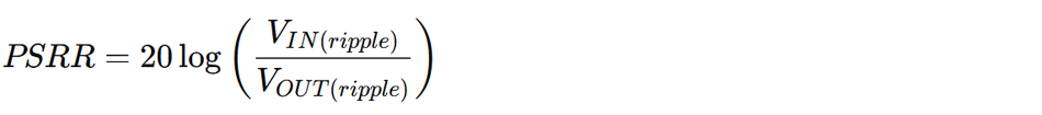
Power Supply Rejection Ratio (PSRR)
PSRR, also called ripple rejection ratio, is the ability of an LDO to suppress ripple on the input or bias voltage. Toshiba defines PSRR as the ratio of input ripple to output ripple expressed in decibels. High PSRR LDOs can attenuate input noise and switching ripple, making them ideal for sensitive analog circuits. For example, the TCR15AG series by Toshiba achieves about 95 dB PSRR at 1 kHz. [2] The TI LP5922 specifies 70 dB PSRR at 1 kHz. PSRR generally decreases with frequency, so measuring it across the relevant range is important.
PSRR is affected by input frequency, ripple amplitude, and load current. High PSRR requires careful design of the error amplifier, pass transistor, and feedback network. Testing PSRR across various frequencies and load conditions yields a complete performance picture.
Line and Load Transient Response
Transient response describes how quickly an LDO responds to rapid changes in input voltage or load current. The fast response requires high loop gain, stable compensation, and appropriate selection of the output capacitor and associated capacitor ESR. Poor load transient response can cause undershoot or overshoot in the output voltage.
Designers should refer to datasheet plots of VOUT versus time for given load steps and ensure the regulator meets system requirements. Devices with fast transient response often use high‑gain error amplifiers and feedforward capacitors.
Protection Features
LDOs incorporate protection circuits such as output current limit and foldback, thermal shutdown, and undervoltage lockout (UVLO).
Output Current Limit prevents excessive output current under fault conditions.
Foldback Protection reduces current further as VOUT collapses, minimizing thermal stress and power loss.
Undervoltage Lockout (UVLO) disables operation when the input voltage falls below a safe threshold.
Thermal Shutdown protects the internal semiconductor die from overheating.
These protection mechanisms are essential in power management systems, particularly in industrial and automotive environments where voltage fluctuations and overload conditions are common.
Recommended Reading: Linear vs Switching Power Supply: Understanding the Differences
External Components and Stability
Importance of External Capacitors
Proper capacitor selection is critical for LDO stability, noise suppression and transient performance. The application notes by Toshiba identify three key capacitors:
Input Capacitor (CIN): Filters noise on VIN and supplies instantaneous current during load steps.
Bias Capacitor (CBIAS): Filters noise on the bias voltage for dual‑supply LDOs and powers internal control circuits.
Output Capacitor (COUT): Supplies instantaneous current to maintain VOUT during load changes and provides phase compensation for the feedback loop.
Most modern LDOs are designed to work with multilayer ceramic capacitors (MLCCs) because they have low ESR and a small size. [3] However, the capacitance of MLCCs varies with applied voltage and temperature; designers must evaluate capacitors across operating conditions to ensure stability. The datasheets specify minimum and maximum capacitance and ESR values required for stable operation.
ESR and ESL Considerations
The equivalent series resistance (ESR) and equivalent series inductance (ESL) of capacitors affect stability and PSRR. High ESR can shift the location of poles and zeros in the LDO’s loop response and cause oscillations. Low‑ESR capacitors such as ceramic MLCCs are preferred, but extremely low ESR can also destabilize some regulators; therefore, always follow the manufacturer’s recommended ESR range.
Engineers emphasize selecting capacitors with low ESL and ESR to maximise PSRR and noise performance. Low ESL capacitors reduce inductive behaviour, improving high‑frequency filtering and loop stability. Criteria for low‑ESL capacitors include choosing MLCCs, high capacitance in small packages, surface‑mount types, and X5R/X7R dielectrics.
Proper PCB layout: placing capacitors close to the regulator pins and minimising via inductance further improves performance.
Recommended Reading: X5R vs X7R: Comprehensive Comparison & Engineering Design Guide
Efficiency and Thermal Considerations
Despite a low dropout regulator provides excellent low-noise and high power supply rejection ratio performance, its efficiency is fundamentally limited by its linear operating principle. Unlike a switching regulator or DC-DC converter, an LDO dissipates the voltage difference between input voltage and output voltage as heat across the pass element (typically a MOSFET or bipolar transistor).

where I(B) represents the quiescent current consumed by the internal control circuitry, including the error amplifier and bias networks.
Designers should calculate P under worst‑case conditions and verify that it is below the regulator’s maximum power dissipation rating. The junction temperature Tj can be estimated using thermal resistance and ambient temperature as:

Proper PCB layout plays a critical role in thermal management. Increasing copper area around the regulator, adding thermal vias, and optimizing ground planes improve heat spreading. If dissipation remains excessive, implementing a step-down converter ahead of the LDO can reduce the effective voltage differential, improving efficiency while preserving the clean output characteristics of the LDO for sensitive analog or mixed-signal loads.
LDO Selection and Application Guidelines
When to Use an LDO Regulator?
Use an LDO regulator when the input voltage is only slightly higher than the required output voltage, the load current is moderate, and low output noise is critical. Typical applications include powering microcontroller cores, RF circuits, audio amplifiers, sensors and precision analog blocks. LDOs are also used after switching converters to clean up switching noise (buck‑followed‑by‑LDO). If efficiency is paramount and the input – output differential is large, a switching regulator may be more appropriate.
Selection Criteria
When choosing an LDO, engineers should evaluate the following criteria:
Criterion | Considerations |
Input Voltage Range | Ensure the minimum VIN, including tolerances and ripple, is higher than VOUT + VDO over all operating conditions. Dual‑supply LDOs may require a bias voltage. |
Output Voltage and Current | Verify that the regulator supports the desired VOUT and maximum load current. Some LDOs have fixed outputs while others are adjustable via external resistors. |
Dropout Voltage | Choose a device with sufficient headroom for the worst‑case load current. Lower dropout improves efficiency and allows operation from lower input rails. |
Quiescent Current | Important for battery‑powered devices and always‑on rails. Ultra‑low IQ LDOs help extend battery life. |
PSRR and Noise | High PSRR and low output noise are essential for analog, RF and high‑speed digital circuits. Check PSRR versus frequency and noise spectral density. |
Load and Line Regulation | Small values indicate that the regulator maintains output accuracy under variations. |
Protection Features | Evaluate overcurrent limit, foldback, thermal shutdown and UVLO thresholds for reliability. |
Package and Thermal Characteristics | Ensure the package can dissipate the expected power. Small packages may require careful thermal design. |
Measurement and Layout Best Practices
Designers should measure PSRR and noise under realistic operating conditions. It is recommended to test PSRR across relevant frequency ranges, using ripple amplitudes representative of real conditions, and to measure under various load currents. Measurement setups should minimise additional noise from cables and signal generators.
For PCB layout, place input, bias and output capacitors as close as possible to the LDO pins to reduce parasitic inductance. Use solid ground planes and short traces. If a feedforward or noise reduction capacitor is recommended, follow the guidelines from the manufacturer.
Recommended Reading: PCB Layout: A Comprehensive Guide
Practical Implementation Example
To illustrate LDO regulator selection and design, consider powering a 1.8 V core rail of an FPGA from a 3.3 V supply with a maximum load current of 1 A. [4] The design goals are to minimise noise, achieve high efficiency, and ensure the regulator remains stable across temperature and load variations.
Device Selection
The target requirements are input voltage ≈ 3.3 V, output voltage = 1.8 V, and output current up to 1 A. The candidate selection should start with datasheets and focus on dropout voltage, power supply rejection ratio, noise, stability requirements, and protection features.
The suitable option is LP5922 by Texas Instruments, a linear regulator capable of high output current with low noise. TCR15AG series by Toshiba, prioritizes high PSRR and it might be attractive when input ripple must be strongly attenuated. If the system includes a noisy upstream step-down stage, selecting a low dropout regulator with strong rejection across relevant high frequencies becomes more important than headline 1 kHz PSRR alone.
Efficiency and Power Loss
For a linear voltage regulator, efficiency is approximately:
With VIN = 3.3 V and VOUT = 1.8 V:

Power dissipation is dominated by the voltage drop across the pass device:


That level of power loss can create a large temperature rise depending on package and layout. If thermal margin is limited, place a DC-DC converter (buck) ahead of the LDO to reduce the voltage differential.
For example, stepping down to 2.0 V and then regulating to 1.8 V reduces LDO dissipation to ~0.2 W and improves overall power consumption, while preserving the low-noise output of LDO.
Setting the Output Voltage
The adjustable LDOs use an external resistor divider to set VOUT. For example, with the LP5922, the output voltage is set by:
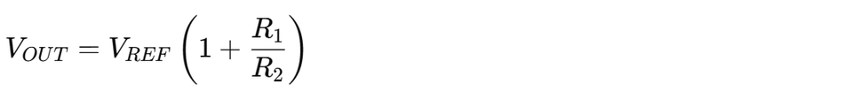
Here, V (REF) is typically 0.5 V. Choosing R2 = 10 kΩ and R1 = 26 kΩ yields V(OUT) ≈ 1.8 V. Always consult the datasheet for recommended resistor values and ensure the divider current is sufficient relative to the device’s reference and feedback input current.
Capacitor Selection and Layout
The LP5922 datasheet specifies a minimum input capacitance of 10 µF and an output capacitance of 47 µF (ceramic) for stability. A small noise reduction capacitor on the SS/NR pin further reduces output noise. Place capacitors close to the regulator pins, use short traces, and use a solid ground plane. For high‑frequency noise suppression, parallel capacitors of different values can extend PSRR across the frequency range. Choose capacitors with low ESR and ESL and verify their effective capacitance under bias.
Pass Device and Architecture Notes
In many regulator ICs, the pass device is a MOSFET (a type of FET) or bipolar transistor. The internal error amplifier drives the pass device (via gate voltage for MOSFET designs) to keep V (OUT) constant. Single-supply architectures are simpler; dual-supply variants can achieve lower dropout and stronger performance at high current, but require additional bias rails.
Recommended Reading: How Do MOSFETs Work: Comprehensive Technical Guide for Engineers
Advanced Architectures and Trends
High‑Bandwidth and Digital LDOs
As chip geometries shrink and supply voltages decrease, conventional analog error amplifiers struggle to deliver high PSRR and fast transient response across wide frequency bands. High‑bandwidth LDO designs add internal gain stages, adaptive compensation or feedforward paths to enhance PSRR at higher frequencies. Some regulators integrate multiple power‑transistor stages to spread the load current and reduce output impedance.
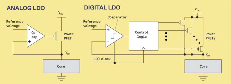
Digital LDOs (DLDOs) are emerging for on‑chip voltage regulation in advanced CMOS processes. Instead of a continuous analog control loop, DLDOs use a digital controller that activates or deactivates a bank of small power transistors (current sources) based on the quantised difference between VOUT and the reference. DLDOs can achieve fine granularity and fast response, making them suitable for delivering low‑voltage supplies within microprocessors and SoCs. However, quantisation can introduce limit‑cycle oscillations and requires careful design of the digital control algorithm and filtering.
Improving PSRR and Noise
Techniques to enhance PSRR include using cascaded error amplifiers, implementing feedforward capacitors, and minimising parasitic resistance and inductance. Some regulators provide an external noise reduction (NR) pin that allows a capacitor to filter the reference voltage and improve low‑frequency PSRR. Advanced devices integrate differential error amplifiers and internal charge pumps to maintain high PSRR with low dropout.
Integration and Package Innovations
Modern LDOs often include additional features such as programmable soft‑start, power‑good indicators, and digital interfaces (I²C, PMBus) that allow dynamic control and monitoring. Package technology (e.g., WSON and flip‑chip) enhances thermal performance and reduces footprint. For high‑current LDOs, packages with exposed thermal pads enable efficient heat spreading.
Recommended Reading: Power Management for Tomorrow’s Innovations
Conclusion
LDO regulators remain indispensable components for providing clean, precise power to digital and analog systems. By understanding fundamental concepts such as dropout voltage, line and load regulation, quiescent current, noise, and PSRR, engineers can effectively select and design with LDOs. Careful attention to capacitor selection and PCB layout ensures stability and high PSRR, while thermal calculations prevent overheating. Practical examples show how to evaluate efficiency, compute power dissipation, and select suitable devices such as the LP5922 or TCR15AG. Looking ahead, high‑bandwidth and digital LDO architectures will continue to push performance boundaries, enabling low‑noise regulation in shrinking silicon nodes. Engineers who grasp these principles will be well equipped to deliver robust power supplies in their next design.
Frequently Asked Questions (FAQ)
Q. What is a low‑dropout (LDO) regulator?
A. An LDO regulator is a linear voltage regulator that maintains regulation with a small input–output voltage differential. Regulators with dropout voltages below about 1 V are classified as LDOs. They use MOSFET pass elements to achieve low dropout, low noise, and fast transient response.
Q. How is dropout voltage defined, and why is it important?
A. Dropout voltage (VDO) is the minimum difference between the input and output required to keep the regulator in regulation. For MOSFET‑based LDOs, VDO equals the product of on‑resistance and output current. Lower dropout allows operation at lower input rails and improves efficiency, especially in battery‑powered systems.
Q. When should I use an LDO instead of a switching regulator?
A. Use an LDO when the input voltage is only slightly higher than the required output voltage, when output noise and PSRR are critical, or when circuit simplicity and small size outweigh efficiency. Combine a switching converter with an LDO when you need both high efficiency and low noise.
Q. What is PSRR, and how is it measured?
A. Power‑supply rejection ratio (PSRR) quantifies the ability of an LDO to suppress input voltage ripple. It is calculated as 20·log10(VIN ripple/VOUT ripple). Measurement involves injecting a known ripple onto the input and measuring the resulting ripple on the output over the frequency range of interest. High PSRR indicates that the regulator effectively attenuates input noise.
Q. How can I reduce noise in an LDO‑powered system?
A. Select an LDO with low output noise and high PSRR; use input, bias and output capacitors with low ESR/ESL and follow the manufacturer’s recommendations; place capacitors close to the device; and consider adding a noise reduction capacitor if available. Also, minimise load‑induced noise by decoupling critical loads and ensuring stable operation across load steps.
Q. What is the role of the bias pin on some LDOs?
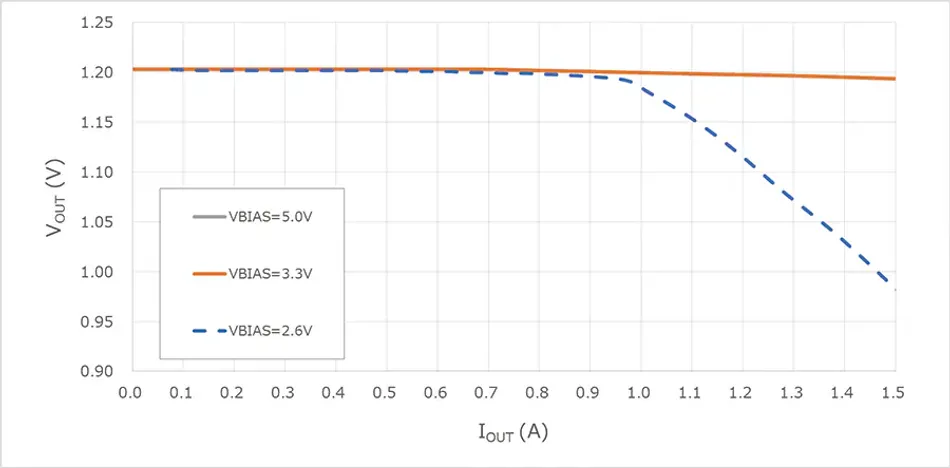
A. Dual‑supply LDOs use a separate bias voltage (VBIAS) to drive the gate of an N‑channel MOSFET. This reduces the on‑resistance and dropout voltage compared with single‑supply P‑channel designs. A bias supply allows operation from very low input voltages but adds complexity since two supplies are required.
References
[1] Texas Instruments. LP5922 2-A Low-Noise, Adjustable LDO With Low Input [Cited 2026 February 12]; Available at: Link
[2] Toshiba. LDO Regulator TCR15AG [Cited 2026 February 12]; Available at: Link
[3] Toshiba. Basics of Low-Dropout (LDO) Regulator ICs [Cited 2026 February 12]; Available at: Link
[4] Analog Devices. Dual Output Supply Powers FPGAs from 3.3V and 5V Inputs [Cited 2026 February 12]; Available at: Link
in this article
1. Key Takeaways2. Introduction3. Fundamentals of LDO Regulators4. Key Parameters and Performance Metrics5. External Components and Stability6. Efficiency and Thermal Considerations7. LDO Selection and Application Guidelines8. Practical Implementation Example9. Advanced Architectures and Trends10. Conclusion11. Frequently Asked Questions (FAQ)12. References