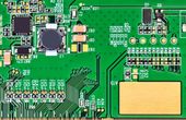
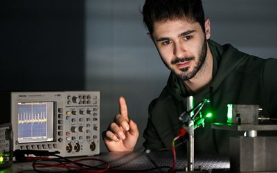
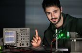
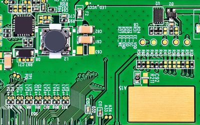
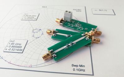
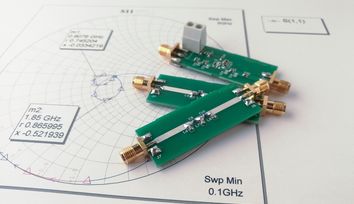
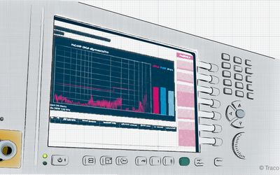
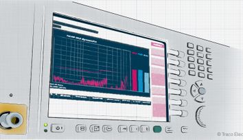
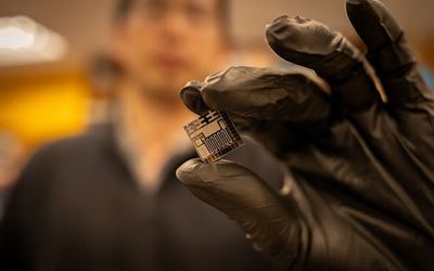
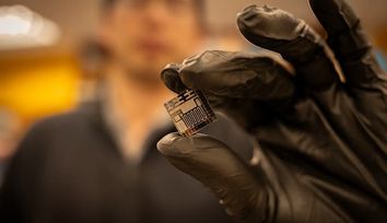
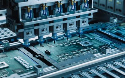
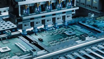
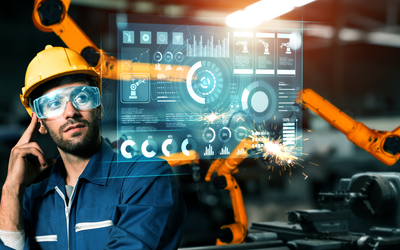
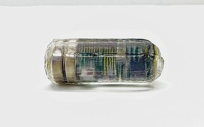
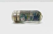
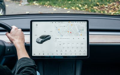
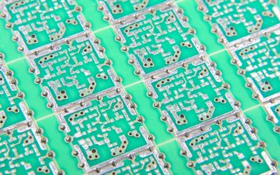
As microLEDs inevitably shrink in size, the micro-bumping requirements for the microLED dies becomes more challenging. Direct wafer-based printing based on gravure offset techniques offers a promising solution in this regard. Indeed, this is another field where printed electronics can play a role.
The three themes are closely linked since QDs can be digitally printed as color conversation materials atop blue microLEDs to enable wide color gamut RGB uLED displays without requiring a separate transfer step for each color.. This is an important technology as it simplifies the manufacturing step for microLED and thus removing a major hinderence.
This article explores transistor circuit design for digital design engineers, hardware engineers, and electronics engineering students. Find out the theoretical foundations with practical guidance, enabling you to confidently build and analyze analog and digital transistor circuits.
This article covers every aspect of the Arduino UNO pinout, presenting a technical, pin-by-pin explanation to help readers confidently design, analyze, and implement Arduino-based systems.
This article explores how to read resistor color code correctly, covering the fundamental theory, relevant standards, practical examples, and design-oriented insights, providing practical tips for efficient and accurate circuit prototyping.
Miniature RFID tags by Murata enable seamless system integration with durable, reprogrammable identification — delivering reliable tracking, authentication & traceability beyond the limits of traditional barcodes.
In this episode, we talk about the engineers that built a wireless tag that detects and remembers overheating without a chip or a battery, enabling cold-chain monitoring without creating electronic waste.
By stacking multiple active components based on new materials on the back end of a computer chip, this new approach reduces the amount of energy wasted during computation.
Focused laser-like light that covers a wide range of frequencies is highly desirable for many scientific studies and for many applications, for instance quality control of manufacturing semiconductor electronic chips.
As microLEDs inevitably shrink in size, the micro-bumping requirements for the microLED dies becomes more challenging. Direct wafer-based printing based on gravure offset techniques offers a promising solution in this regard. Indeed, this is another field where printed electronics can play a role.
The three themes are closely linked since QDs can be digitally printed as color conversation materials atop blue microLEDs to enable wide color gamut RGB uLED displays without requiring a separate transfer step for each color.. This is an important technology as it simplifies the manufacturing step for microLED and thus removing a major hinderence.
PCB layers are the copper layers within a printed circuit board, laminated between or onto layers of conductive material. These layers are stacked to enhance the functionality of electronic devices. This article explores the concept of PCB layering, the various types of layers, and their benefits.
In this article, we look at how Super Low power Wi-Fi and Bluetooth LE enable smart locks to be more agile and reliable by demonstrating these features with a case study from Renesas.
The EVT Stage implements the design in its form, fit, and function to better inform stakeholders of your production intent. Don't rush this important milestone.
Flexible electronics have enabled the design of sensors, actuators, microfluidics and electronics on flexible, conformal and/or stretchable sublayers for wearable, implantable or ingestible applications.
Article #3 of the Enabling IoT Series. This article looks at how Time of Flight (ToF) sensors are used for this purpose and are changing the way we can interact with VR, and other video technologies.
Canadian researchers have discovered that they can stick hydrogel plasters to the skin very effectively using ultrasound. Outi Supponen has now explained the underlying mechanism: imploding bubbles that form within the adhesive located between the plaster and the skin anchor the one on the other.
Magnetism is a force exerted by charged particles in motion that allows them to attract/repel other moving charged particles. The universal phenomenon is responsible for shaping the world as we know it.
Phosphors or QDs for color conversion in LCD and microLED ? Which will win? This is an evolving technology space to watch. Here, it is shown that phosphor technology is evolving, enabling not just red but also green narrowband color conversation with small particle sizes compatible with microLEDs
Molecular particle free inks can offer extreme formability and stretchability, allowing the design and production of 3D shaped and/or in-mold electronics parts with extreme curvatures and complex shapes.