PCB Trace: The Backbone of Modern Circuit Design
PCB traces are fundamental components in circuit design, serving as the pathways for electrical signals. This article examines the advancements, applications, and challenges of PCB trace technology. Discover insights into optimizing designs and overcoming common obstacles in PCB trace implementation.

Last updated on 25 Jun, 2024. 21 minutes read
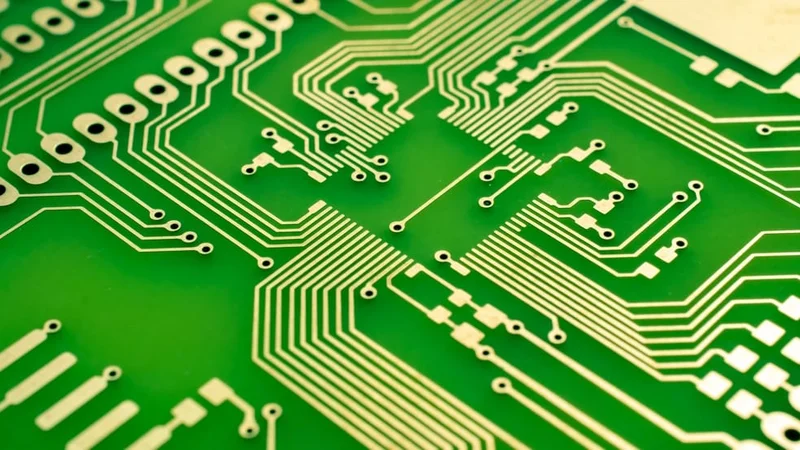
The layout of Traces on a PCB
Introduction
PCB trace technology is a cornerstone of modern electronic design, forming the intricate pathways that connect components on a printed circuit board (PCB). These conductive tracks ensure electrical signals are transmitted accurately and efficiently throughout the circuit. The design and quality of PCB traces can significantly influence the performance, reliability, and functionality of electronic devices.
In engineering projects, PCB traces play a critical role in defining the electrical characteristics of a circuit. Proper trace design can minimize signal loss, reduce electromagnetic interference, and enhance thermal management, leading to more robust and efficient systems. As electronic devices become more compact and complex, the precision and innovation in PCB trace technology become increasingly crucial, impacting everything from consumer electronics to advanced industrial systems. Proper PCB assembly techniques are essential to ensure that these intricate traces are correctly connected and functioning optimally, ensuring the overall performance and reliability of the electronic device.
Unveiling the Basics of PCB Traces
PCB engineers and designers must grasp the basics of PCB traces to craft high-performance printed circuit boards. Understanding trace width, layout, and material properties is essential for optimizing signal integrity, minimizing electromagnetic interference, and ensuring thermal management. Mastery of these basics leads to reliable, efficient, and cutting-edge electronic designs that meet the rigorous demands of modern technology. Here are some basics:
Key Concepts and Components
Understanding the fundamental components of a trace PCB is essential for grasping how these intricate circuits function. Here are the main components:
Traces: Traces are conductive pathways etched onto the PCB substrate, usually made of copper for its excellent conductivity and durability. They revolutionized electronics by replacing cumbersome point-to-point wiring with standardized, reliable pathways. These paths are meticulously designed with specific widths and thicknesses to handle different current levels and maintain signal integrity. Advancements like high-density interconnect (HDI) technologies enable even more intricate and compact designs.
Pads: Pads are exposed areas of copper where components are soldered. They come in two main types: through-hole pads, for components with leads that pass through the board, and surface-mount pads, for components mounted directly onto the PCB surface. Pads are crucial for ensuring stable connections and optimal conductivity. Advances in SMT have significantly increased the efficiency and reliability of modern electronics manufacturing.
Vias: Vias are plated through-holes that enable electrical connections between different layers of a multi-layer PCB, allowing for complex circuits that require vertical signal routing. They can be through-hole, blind (connecting outer to inner layers), or buried (connecting inner layers without reaching outer surfaces). Microvias in HDI PCBs have enabled further miniaturization and complexity.
Recommended reading: What are Vias in Pad? Advantages, Limitations, Applications, and Comparison with Conventional Vias
The Purpose and Function of PCB Traces
PCB traces are essential pathways for electrical signals between components in electronic circuits. Made of conductive tracks, typically copper, etched onto a non-conductive substrate, they ensure efficient and reliable signal transmission critical for device performance. Traces interconnect components like resistors, capacitors, and integrated circuits, allowing circuits to function correctly. For example, in an amplifier circuit, traces connect the power supply, input signal, transistors, and output to ensure proper signal amplification.
The demand for compact, reliable, and efficient devices has driven PCB trace technology evolution from labor-intensive point-to-point wiring to advanced PCB designs using materials like FR4. Modern smartphones, for instance, rely on precisely designed traces for high-speed data transmission without interference, ensuring overall performance and reliability. Flaws in trace design can lead to poor performance or device failure.
Materials and Construction of PCB Traces
PCB traces are predominantly made from copper due to its excellent electrical conductivity and thermal characteristics. Copper ensures minimal resistive losses, maintaining signal integrity and efficient power distribution. Its ability to dissipate heat effectively is crucial for high-power and high-frequency applications.
The construction of PCB traces involves several critical manufacturing processes. Photolithography is one common method, where a photoresist layer on a copper-clad board is exposed to ultraviolet light through a photomask, creating a patterned layout that is etched into the copper layer. Electroplating is another essential process, increasing copper trace thickness and adding other conductive layers, enhancing electrical properties and mechanical durability.
Several factors affect PCB trace quality and reliability. Copper thickness, ranging from 0.5 oz/ft² to 2 oz/ft², impacts current-carrying capacity and thermal performance. Surface finishes, such as hot air solder leveling (HASL), immersion gold, and organic solderability preservatives (OSP), influence solderability and corrosion resistance.
While copper remains the gold standard for PCB traces due to its conductivity, thermal performance, and cost-effectiveness, alternative materials like aluminum and silver are used in specialized applications. Aluminum is favored in power electronics for its lightweight and thermal conductivity, while silver is used in high-frequency circuits for its superior conductivity despite its higher cost.
Understanding these materials and construction processes is crucial for designing high-performance PCB traces in advanced electronic applications.
Design Considerations for Effective PCB Traces
Designing PCB traces involves several critical considerations that directly impact the performance and reliability of the circuit. Key factors such as trace width, spacing, and layout must be carefully managed to ensure optimal signal integrity and overall system performance.
Trace Width
The width of a PCB trace is a fundamental parameter that affects its current-carrying capacity and resistance. Wider traces can handle higher currents with lower resistance, crucial for power delivery and minimizing voltage drops. Conversely, narrower traces are suitable for signal lines where high current isn't required. However, they must be designed to avoid excessive resistance that could degrade signal quality. According to IPC-2221 standards, minimum trace widths are dictated by current requirements and thermal management needs, which include ambient temperature. A higher ambient temperature necessitates wider traces to ensure safe operation and prevent overheating due to increased resistance. By carefully considering trace width, designers balance current capacity, signal integrity, and thermal performance within the limitations set by the PCB's environment.
Trace Spacing
Trace spacing, or the distance between adjacent traces, is vital for preventing crosstalk and electromagnetic interference (EMI). Adequate spacing helps maintain signal integrity by reducing the coupling of electromagnetic fields between traces. This is especially important in high-frequency circuits where signal interference can lead to data corruption and performance issues. Historically, as operating frequencies increased, design practices evolved to incorporate greater spacing to combat these challenges, guided by standards such as IPC-2221 and IPC-2141.
Layout Considerations
The overall layout of PCB traces involves strategic planning to optimize the routing of signals and power lines. Effective layout design minimizes signal path lengths, reduces the potential for interference, and enhances thermal management. Designers must also consider the placement of components to ensure efficient connectivity and maintain the board's mechanical stability. The evolution of PCB layout techniques reflects advancements in electronic design automation (EDA) tools, which have significantly improved the ability to create complex and precise layouts.
Below is a table comparing different design parameters and their effects:
Parameter | Impact on Performance | Recommendations |
Trace Width | Affects current-carrying capacity and resistance | Use wider traces for power lines, narrower ones for signals |
Trace Spacing | Prevents crosstalk and EMI | Maintain adequate spacing based on signal frequency |
Trace Layout | Optimizes signal routing and thermal management | Minimize signal path lengths, consider thermal paths |
These design considerations are crucial for creating effective PCB traces that ensure reliable signal transmission and robust performance. By carefully managing trace width, spacing, and layout, designers can mitigate common issues such as signal degradation and interference, leading to more efficient and reliable electronic circuits.
Cutting-Edge Developments in PCB Trace Technology
The cutting-edge advancements in trace PCB materials have unlocked a new era of possibilities for even smaller, faster, and more powerful devices. Below are some of them:
Advanced Materials for PCB Traces
The quest for improved performance and miniaturization in electronic devices has led to the exploration of advanced materials for PCB traces. Among these, graphene, conductive polymers, and advanced alloys are at the forefront, offering unique properties that surpass traditional copper in several aspects.
Graphene is a single layer of carbon atoms arranged in a two-dimensional lattice. Its discovery in 2004 marked a significant breakthrough in material science, earning the Nobel Prize in Physics in 2010. Graphene boasts exceptional electrical conductivity, thermal conductivity, and mechanical strength. Its electron mobility is significantly higher than copper, making it an ideal candidate for high-frequency and high-speed applications. The thermal conductivity of graphene helps in efficient heat dissipation, crucial for high-power circuits. Currently, graphene is being implemented in flexible electronics and transparent conductive films, leveraging its flexibility and conductivity. However, large-scale production and integration into existing manufacturing processes remain significant challenges, limiting its widespread adoption.
Conductive polymers, such as polyaniline and PEDOT, are an emerging material for PCB traces, first developed in the late 1970s. These polymers are lightweight and flexible, with tunable electrical properties through chemical doping. They are ideal for applications like flexible displays and wearable electronics where traditional rigid PCBs are impractical. Despite their lower conductivity compared to metals and stability issues over long-term use, ongoing innovations in polymer chemistry are enhancing their performance, making them increasingly viable for high-demand applications.
Advanced alloys are another promising material for PCB traces. These alloys, such as copper-nickel and copper-tungsten, are being explored to enhance the performance of PCB traces. These alloys combine the high conductivity of copper with the additional benefits of other metals, such as improved thermal stability and mechanical strength. Copper-nickel alloys, for instance, have been used since the 1960s in environments with high thermal stress, while copper-tungsten alloys are employed in applications requiring high wear resistance and thermal conductivity. The use of these alloys in aerospace and military applications highlights their robustness and reliability. Continuous advancements in metallurgical processes are enhancing the properties of these alloys, making them more suitable for modern electronic needs.
Opportunities and Challenges
The implementation of these advanced materials in cutting-edge applications showcases their potential to revolutionize PCB technology. For example, the use of graphene in flexible circuits for medical devices allows for more compact and efficient designs. Conductive polymers are being used in developing lightweight, foldable smartphones, pushing the boundaries of traditional electronic design. Advanced alloys, with their enhanced durability and conductivity, are critical in high-reliability applications such as satellite communications and military hardware.
Despite their promising properties, these advanced materials face practical challenges that hinder widespread adoption. Graphene's production costs and integration complexity need to be reduced for it to be viable on a commercial scale. Conductive polymers require improvements in conductivity and stability to match the performance of metallic traces. Advanced alloys, while offering superior properties, often involve more complex manufacturing processes and higher costs.
Incorporating these advanced materials into PCB traces represents a significant leap forward in electronic design, offering pathways to more efficient, durable, and versatile devices. However, overcoming the associated challenges will be crucial to fully realize their potential and integrate them into mainstream manufacturing processes.
Innovations in PCB Design Software
The evolution of PCB design software has revolutionized the way engineers create and optimize circuit boards. These tools have become indispensable, offering advanced features that significantly enhance trace design and overall board performance.
Modern PCB design software includes several key advancements:
Automated Routing: Automated routing algorithms have become increasingly sophisticated, enabling the efficient layout of complex traces with minimal manual intervention. These algorithms can optimize trace paths for signal integrity and thermal management, reducing design time and improving reliability.
Signal Integrity Analysis: Signal integrity (SI) tools integrated into PCB design software allow engineers to simulate and analyze how signals will behave in the actual physical layout. These tools help identify and mitigate issues such as crosstalk, reflection, and electromagnetic interference (EMI), ensuring that high-speed signals are transmitted accurately.
Thermal Simulation: As electronic devices become more compact and powerful, managing heat dissipation is crucial. PCB design software now includes thermal simulation capabilities that allow designers to predict and manage heat flow within the board, optimizing the placement of components and traces to prevent overheating.
Here are some popular PCB design software tools and their key features:
Altium Designer:
Comprehensive design environment with integrated schematic capture, PCB layout, and 3D visualization.
Advanced routing tools with interactive and automated features.
Robust SI analysis and real-time design rule checking.
Extensive library of components and footprints.
Cadence Allegro PCB Designer:
High-performance design tools for complex, high-speed PCBs.
Advanced routing and constraint-driven design features.
Integrated SI, power integrity (PI), and thermal analysis tools.
Collaboration capabilities with team design and concurrent engineering.
Mentor Graphics PADS:
User-friendly interface with powerful design and layout tools.
Comprehensive SI and PI analysis capabilities.
Thermal analysis and management tools.
Integrated library management and component sourcing.
Autodesk Eagle:
Cost-effective solution with schematic capture and PCB layout capabilities.
Flexible design rules and real-time error checking.
Integration with Fusion 360 for mechanical design collaboration.
Extensive community support and library of components.
KiCad:
Open-source and free PCB design suite.
Feature-rich environment with schematic capture, PCB layout, and 3D viewer.
Community-driven development with regular updates and enhancements.
Comprehensive library support and custom footprint creation.
Modern Manufacturing Techniques
Recent advancements in PCB manufacturing processes have significantly enhanced trace performance and reliability, catering to the growing demand for precision and miniaturization in modern electronics. Understanding the historical context and fundamental principles behind these techniques provides deeper insight into their significance and application.
High-Density Interconnect (HDI) PCBs
HDI PCBs represent a leap forward in PCB technology, allowing for more components in a smaller area. This innovation dates back to the late 1980s when the electronics industry sought ways to integrate more functionality into increasingly compact devices. HDI boards utilize microvias, finer lines and spaces, and high-performance materials to achieve superior electrical performance and reliability. HDI technology can be seen in modern smartphones and tablets, where space constraints demand high-density interconnects to fit more functionality into thinner profiles.
HDI PCBs pack a punch with miniaturized components and intricate circuitry. However, this miniaturization brings its own set of challenges. Trace resistance, measured in ohms, becomes a critical factor. Thinner traces, a consequence of shrinking size, can lead to higher resistance, hindering efficient signal transmission and causing power loss. Balancing trace resistance with amp capacity is crucial. Ensuring adequate amperage allows for safe operation and prevents overheating due to excessive current. In high-frequency applications, managing changes in resistance across the PCB is essential to maintain signal integrity and prevent unwanted interference. By carefully considering these factors – trace resistance, amp, and ohm management – designers can optimize HDI PCB performance, making them a vital component in modern electronics.
The HDI manufacturing process involves several critical steps:
Design and Material Selection: HDI boards require meticulous design to ensure optimal placement of microvias and fine traces. High-performance materials like polyimide are often used.
Laser Drilling: Microvias, which are much smaller than traditional vias, are drilled using precision lasers. These microvias can connect multiple layers, enabling complex routing in a compact space.
Electroless Plating: After drilling, the microvias are plated using an electroless copper deposition process to ensure reliable electrical connections between layers.
Sequential Lamination: Multiple layers are laminated sequentially, allowing for the integration of complex layer stacks that enhance performance and reliability.
Recommended reading: PCB Via: What is a Via?
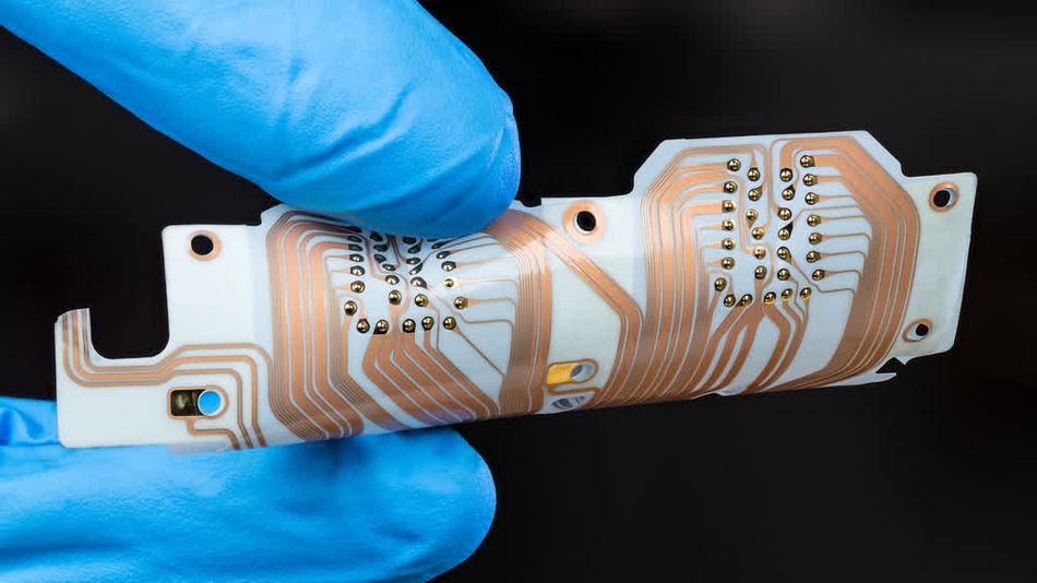
Flexible PCBs
Flexible PCBs offer unparalleled versatility, allowing circuits to bend and fold without compromising performance. The concept of flexible electronics dates back to the 1960s, driven by the need for compact and adaptable circuit designs in military and aerospace applications. Today, these are increasingly used in wearable technology, medical devices, and other applications where space and flexibility are critical.
The manufacturing process for flexible PCBs includes:
Substrate Preparation: Flexible substrates, typically made from polyimide, are prepared. These materials offer excellent flexibility and thermal stability.
Circuit Patterning: The circuit patterns are created using photolithography, similar to rigid PCBs, but with techniques adapted to flexible substrates.
Etching and Plating: Copper is etched to form the circuit traces, followed by plating processes to enhance electrical conductivity and reliability.
Coverlay Application: A flexible coverlay is applied to protect the circuit traces and enhance mechanical durability.
Component Assembly: Surface mount technology (SMT) is used to place solder components onto the flexible substrate, ensuring robust connections even under flexing conditions.
Recommended reading: Flexible and Printed Electronics: Breakthroughs, Applications, and Challenges
Additive Manufacturing (3D Printing)
Additive manufacturing, or 3D printing, is revolutionizing PCB production by enabling the creation of complex geometries that are impossible with traditional methods. Originating from the rapid prototyping industry in the 1980s, this technique allows for rapid prototyping and customization, significantly reducing time-to-market. Applications of 3D-printed PCBs include custom medical devices and small-batch production of specialized electronic components, where rapid iteration and customization are paramount.
The additive manufacturing process for PCBs involves:
3D Design and Modeling: The PCB design is created using advanced CAD software, allowing for intricate and customized layouts.
Material Deposition: Conductive inks and dielectric materials are deposited layer by layer using precision 3D printers. This allows for the creation of complex multilayer circuits in a single printing process.
Curing and Sintering: Each layer of material is cured or sintered to ensure structural integrity and electrical conductivity. This step is crucial for achieving reliable and durable traces.
Component Placement and Soldering: Components are placed and soldered onto the 3D-printed substrate using traditional or specialized techniques adapted for 3D-printed surfaces.
Recommended reading: Gaining an Understanding of the Impacts of Additive Manufacturing
These modern manufacturing techniques are pushing the boundaries of what is possible in PCB design and production. By leveraging HDI, flexible PCBs, and additive manufacturing, engineers can achieve unprecedented levels of precision, reliability, and miniaturization, meeting the ever-increasing demands of advanced electronic applications.
Real-World Applications of Advanced PCB Traces
1. Enhancing Signal Integrity in High-Speed Circuits
Historically, the challenges of signal integrity emerged with the advent of high-speed digital circuits in the late 20th century. Engineers developed several techniques to address these issues, which have since become standard practice in high-speed PCB design. Signal integrity refers to the preservation of electrical signal quality and reliability as they traverse PCB traces. At higher frequencies, signals are more susceptible to degradation due to electromagnetic interference (EMI), crosstalk, and reflection.
Differential signaling is a key technique to combat EMI and crosstalk by using pairs of traces carrying equal and opposite signals, canceling out noise. This method is now standard in high-speed communication protocols like USB, HDMI, and Ethernet.
Controlled impedance traces are essential as signal frequencies increase. Consistent impedance minimizes reflections and signal degradation, achieved by designing trace width, spacing, and the dielectric properties of the PCB material. Modern high-frequency applications, such as RF and microwave circuits, rely heavily on controlled impedance designs.
Proper grounding techniques enhance signal integrity by providing a low-impedance return path for current and shielding against EMI. Effective strategies include using solid ground planes, implementing ground vias, and referencing signal traces to these ground planes.
In high-speed data centers, differential signaling and controlled impedance maintain signal integrity over extensive networks. Advanced routers and switches handle vast amounts of data without loss or corruption. In the automotive industry, advanced driver-assistance systems (ADAS) use these techniques to ensure accurate and timely data communication between sensors and processing units.
Recommended reading: How Advanced Driver-Assistance Systems (ADAS) Impact Automotive Semiconductors
By implementing these techniques, engineers can design high-speed PCBs that preserve signal integrity, ensuring reliable and efficient operation in complex electronic systems.
2. Optimizing Power Delivery in Complex Systems
Efficient power delivery is a critical aspect of PCB design, ensuring that all components receive the necessary voltage and current to operate correctly. PCB traces play a fundamental role in this process, acting as the conduits for electrical power across the board.
Role of PCB Traces in Power Delivery
PCB traces must be designed to handle significant current loads without excessive voltage drops or heat generation. The width, thickness, and layout of these traces determine their ability to deliver power efficiently. If not properly designed, power traces can introduce resistance that leads to voltage drops, potentially affecting the performance and stability of the components they supply.
Strategies for Designing Power Traces
Minimizing Voltage Drops: To minimize voltage drops, power traces should be wide enough to carry the required current without generating excessive resistance. The IPC-2221 standard provides guidelines for calculating the appropriate trace width based on the current load and acceptable temperature rise. Additionally, using thicker copper layers can reduce resistance further, especially in high-current applications.
Reducing Electromagnetic Interference (EMI): EMI can disrupt the operation of sensitive components and degrade overall system performance. To mitigate EMI, power traces should be routed away from signal traces and sensitive analog components. Implementing ground planes and using decoupling capacitors at strategic locations can also help filter out noise and stabilize voltage levels.
Managing Heat Generation: Heat generation in power traces is a byproduct of electrical resistance. Effective thermal management involves designing traces that dissipate heat efficiently. This can be achieved by spreading the current load across multiple layers using vias to connect these layers, thus distributing heat more evenly. Heat sinks and thermal vias can also be incorporated to enhance heat dissipation from high-power areas.
3. Applications in IoT and Wearable Devices
Advanced PCB traces are crucial in the development of Internet of Things (IoT) and wearable technologies, where size, flexibility, and performance are paramount. These devices often operate in challenging environments, requiring innovative solutions to ensure reliability and functionality.
Unique Challenges and Solutions for Miniaturized, Flexible PCBs
Challenges:
Miniaturization: IoT and wearable devices require extremely compact PCBs, which can lead to issues with heat dissipation and signal integrity.
Flexibility: Wearable devices often need to conform to various shapes and movements, demanding flexible PCBs that maintain performance without compromising durability.
Power Efficiency: These devices typically rely on limited power sources, necessitating highly efficient power management solutions.
Solutions:
Advanced Materials: The use of materials like polyimide and flexible laminates allows for durable, flexible PCBs that can withstand repeated bending and twisting.
High-Density Interconnect (HDI) Technology: HDI PCBs enable the integration of more components in a smaller area, which is essential for miniaturized devices.
Thermal Management Techniques: Incorporating thermal vias and heat spreaders helps to manage heat dissipation in compact designs.
Power Management ICs: Utilizing specialized power management integrated circuits (PMICs) ensures efficient power usage, extending the battery life of IoT and wearable devices.
Key Applications and Benefits
Fitness Trackers: Advanced PCBs are used to create small, flexible devices that monitor physical activity, heart rate, and other health metrics. The flexibility and durability of these PCBs allow the devices to be worn comfortably on the wrist, even during vigorous activities.
Smartwatches: These wearables integrate multiple functions such as communication, fitness tracking, and health monitoring. The compact and efficient design of advanced PCBs supports the miniaturization required for these multifunctional devices.
Medical Devices: Flexible PCBs are essential in developing medical wearables like continuous glucose monitors and portable ECG monitors. These devices require reliable performance in various conditions, made possible by robust, flexible PCB designs.
Smart Clothing: Embedding flexible PCBs into clothing allows for the integration of sensors and electronic components, enabling features like biometric monitoring and environmental sensing. This application benefits from the PCB’s ability to flex and stretch with the fabric.
IoT Sensors: In smart homes and industrial IoT applications, advanced PCBs are used to create compact, energy-efficient sensors that monitor and communicate environmental data. These sensors often operate in remote or hard-to-reach locations, emphasizing the need for reliable, low-power designs.
Navigating the Challenges of PCB Trace Technology
1. Signal Integrity Issues and Solutions
In high-speed PCB designs, maintaining signal integrity is crucial to ensure the reliability and performance of electronic circuits. Signal integrity issues can lead to data corruption, timing errors, and overall system instability. Common problems include crosstalk, reflection, and ground bounce, each of which requires specific strategies for mitigation.
Crosstalk occurs when a signal on one trace induces an unwanted signal on an adjacent trace, leading to interference and potential data errors. This is particularly problematic in high-density PCBs where traces are closely spaced. To mitigate crosstalk:
Increase Trace Spacing: Ensuring adequate spacing between adjacent traces can significantly reduce crosstalk. The IPC-2221 standard provides guidelines for minimum spacing based on the operating frequency.
Use Guard Traces: Placing a grounded guard trace between high-speed signal traces can help absorb and shield against crosstalk.
Differential Signaling: Using differential pairs, where two traces carry equal and opposite signals, can cancel out crosstalk due to their equal exposure to external noise.
Reflection is caused by impedance mismatches along the signal path, leading to signal reflections that interfere with the original signal. This can result in distorted waveforms and data integrity issues. To mitigate reflection:
Impedance Matching: Ensuring that the characteristic impedance of the trace matches the source and load impedances can minimize reflections. This is achieved by carefully controlling trace width, spacing, and the PCB dielectric material.
Proper Termination: Terminating the signal line with a resistor that matches the characteristic impedance can absorb reflections and prevent them from traveling back along the trace. Common termination techniques include parallel termination and series termination.
Ground Bounce occurs when multiple simultaneous switching outputs cause fluctuations in the ground potential, leading to noise and signal integrity problems. This is often seen in designs with high-speed digital circuits. To mitigate ground bounce:
Use Solid Ground Planes: A continuous ground plane provides a low-impedance return path, reducing the likelihood of ground bounce.
Decoupling Capacitors: Placing decoupling capacitors near power pins of ICs can help stabilize the voltage supply and reduce ground bounce.
Controlled Rise and Fall Times: Slowing down the rise and fall times of switching signals can reduce the simultaneous switching noise, thus mitigating ground bounce.
2. Thermal Management in PCB Design
Thermal management is crucial in PCB design to ensure the reliable performance and longevity of electronic components. As electronic devices become more powerful and compact, the amount of heat generated increases, posing significant challenges for maintaining optimal operating temperatures.
Importance of Thermal Management
Effective thermal management prevents overheating, which can lead to component failure, reduced efficiency, and decreased lifespan of the PCB. High temperatures can cause materials to degrade, solder joints to weaken, and components to malfunction. Thus, implementing robust thermal management strategies is essential to maintain performance and reliability.
Techniques for Effective Thermal Dissipation
Thermal Vias: Thermal vias are small, plated holes that provide a path for heat to transfer from the PCB's surface to internal layers or an external heat sink. These vias are particularly effective in multi-layer boards where heat needs to be dissipated across different layers.
Design Considerations: Thermal vias should be strategically placed near high-heat-generating components. Their number, size, and placement must be optimized to maximize heat transfer without compromising the board's mechanical integrity.
Heat Sinks: Heat sinks are metallic components attached to heat-generating parts of the PCB. They increase the surface area available for heat dissipation, allowing for more efficient cooling.
Types of Heat Sinks:
Passive Heat Sinks: Made of materials like aluminum or copper, these rely on natural convection to dissipate heat. They are suitable for applications with lower heat loads.
Active Heat Sinks: These include fans or blowers to increase airflow and enhance heat dissipation. They are used in high-power applications where passive cooling is insufficient.
Thermal Interface Materials (TIMs): TIMs are substances placed between heat-generating components and heat sinks to improve thermal conduction. They fill microscopic air gaps and irregularities, ensuring better contact and heat transfer.
Types of TIMs:
Thermal Pastes: These are often used in applications where a thin layer is needed to fill gaps and provide efficient thermal conductivity.
Thermal Pads: Made from materials like silicone or graphite, thermal pads are easier to apply and handle, suitable for larger gaps or where paste application is impractical.
Phase Change Materials (PCMs): These materials change state (from solid to liquid) at a specific temperature, enhancing thermal conductivity during high thermal loads.
Comparison of Thermal Management Strategies
Strategy | Advantages | Disadvantages |
Thermal Vias | Efficient heat transfer across layers | May complicate PCB manufacturing |
Passive Heat Sinks | No moving parts, reliable | Limited by natural convection |
Active Heat Sinks | Superior cooling performance | Additional power consumption, noise |
Thermal Pastes | High thermal conductivity, easy to apply thinly | Can be messy, requires precise application |
Thermal Pads | Easy to handle and apply | Lower thermal conductivity compared to pastes |
PCMs | Excellent during peak thermal loads | More complex, can be expensive |
Recommended reading: Next-generation MOSFET technology Meets Demand for Strong Thermal Performance in Automotive Applications
3. Overcoming Manufacturing Constraints
PCB trace manufacturing faces several significant challenges, including miniaturization, yield rates, and material compatibility. These challenges can impact the efficiency, cost, and scalability of PCB production.
Challenges in PCB Trace Manufacturing
Miniaturization: As electronic devices become smaller, the demand for more compact and densely packed PCBs increases. This miniaturization requires extremely fine traces and small components, which can be difficult to manufacture with high precision.
Yield Rates: The complexity of modern PCBs can lead to lower yield rates, meaning a higher percentage of boards may have defects that make them unusable. This affects overall production costs and efficiency.
Material Compatibility: Different materials used in PCBs, such as substrates and conductive layers, must be compatible to ensure reliable performance. Incompatibilities can lead to issues like delamination, poor adhesion, and thermal mismatch.
New Manufacturing Techniques and Materials
Advanced Photolithography: This technique has evolved to allow for finer trace widths and spaces, essential for miniaturization. By using shorter wavelength light sources and improved photoresist materials, manufacturers can achieve higher resolution patterns.
Benefits: Enhanced precision in trace and space dimensions, enabling the production of high-density interconnects (HDI) required for modern electronics.
Laser Direct Imaging (LDI): LDI technology uses laser beams to directly image the PCB pattern onto the photoresist layer. This method bypasses traditional photomasks, reducing the risk of alignment errors and allowing for more intricate designs.
Benefits: Improved accuracy and flexibility in PCB design, better suited for rapid prototyping and low-volume production runs.
Material Innovations: New materials, such as flexible laminates and advanced composite substrates, are being developed to improve compatibility and performance.
Flexible Laminates: These materials allow for the creation of flexible PCBs, which can bend and twist without losing integrity, ideal for wearable and IoT devices.
Advanced Composites: These substrates offer better thermal management and mechanical strength, reducing issues like delamination and improving overall reliability.
Additive Manufacturing (3D Printing): This method is increasingly used for creating complex PCB structures that traditional methods cannot achieve. It allows for precise control over material deposition and layer thickness.
Benefits: Enables the creation of complex, multi-layered designs with embedded components, improving integration and reducing assembly steps.
Enhanced Inspection and Testing Methods: Modern inspection techniques, such as automated optical inspection (AOI) and X-ray inspection, help identify defects early in the manufacturing process, improving yield rates.
Automated Optical Inspection (AOI): Uses cameras and imaging software to detect surface defects and misalignments in PCBs.
X-ray Inspection: Provides a non-destructive way to inspect internal layers and solder joints, identifying hidden defects that could compromise PCB performance.
Common Manufacturing Constraints and Solutions
Constraint: Miniaturization
Solution: Use advanced photolithography and laser direct imaging (LDI) to achieve finer traces and spaces.
Constraint: Yield Rates
Solution: Implement enhanced inspection methods like AOI and X-ray inspection to detect defects early and improve overall production quality.
Constraint: Material Compatibility
Solution: Develop and use innovative materials like flexible laminates and advanced composites to ensure better performance and reliability.
Conclusion
Maintaining expertise in PCB trace technology is crucial for engineering professionals striving to ensure the reliability and performance of modern electronic devices. This article highlights significant advancements, including innovative materials, advanced manufacturing techniques, and effective thermal management strategies, underscoring the dynamic and evolving nature of PCB design. By embracing these advancements and understanding the complexities of signal integrity and power delivery, engineers can optimize their designs to meet the growing demands of high-speed, miniaturized, and multifunctional electronic applications. Staying informed about these technological developments is essential for maintaining a competitive edge and achieving excellence in electronic design. As the industry progresses, continuous learning and adaptation will be key to pushing the boundaries of what is possible in electronic innovation.
Frequently Asked Questions
Q1: What are PCB traces and why are they important?
PCB traces are the conductive pathways that connect different components on a printed circuit board (PCB). They are crucial for transmitting electrical signals and power throughout the board, ensuring that the electronic device functions correctly.
Q2: What materials are commonly used for PCB traces?
Copper is the most commonly used material for PCB traces due to its excellent electrical conductivity and thermal properties. Other materials like graphene, conductive polymers, and advanced alloys are also being explored for specialized applications.
Q3: How do you ensure signal integrity in high-speed PCB designs?
Maintaining signal integrity in high-speed PCB designs involves several techniques, including differential signaling, controlled impedance traces, and proper grounding. These methods help minimize issues like crosstalk, reflection, and electromagnetic interference (EMI).
Q4: What are the main challenges in PCB trace manufacturing?
Key challenges in PCB trace manufacturing include miniaturization, achieving high yield rates, and ensuring material compatibility. These challenges can affect the efficiency, cost, and scalability of PCB production.
Q5: How can thermal management be improved in PCB design?
Effective thermal management can be achieved through techniques such as using thermal vias, heat sinks, and thermal interface materials. These strategies help dissipate heat and maintain optimal operating temperatures for electronic components.
Q6: What role do advanced manufacturing techniques play in PCB production?
Advanced manufacturing techniques like photolithography, laser direct imaging (LDI), and additive manufacturing (3D printing) allow for finer trace widths, higher precision, and the ability to create complex PCB structures that are not possible with traditional methods.
Q7: How are PCBs used in IoT and wearable devices?
In IoT and wearable devices, PCBs need to be miniaturized and flexible to fit into compact and dynamic environments. Advanced PCB traces are used to ensure these devices are reliable, efficient, and capable of withstanding various conditions.
Reference
Yun Industrial. What are PCB Traces? 2021 Available from: https://yic-assm.com/what-are-pcb-traces/ (Accessed on June 21, 2024).
Auto Desk. Everything You Need to Know About Trace Width, 2021. Available from: https://www.autodesk.com/products/fusion-360/blog/trace-width/#:~:text=For%20typical%20PCBs%2C%20the%20most,be%206mil%20or%200.152mm.(Accessed on June 21, 2024).
Cauwe, Maarten & Vandevelde, Bart & Nawghane, Chinmay & Slyeke, Marnix & Bosman, Erwin & Verhegge, Joachim & Coulon, Alexia & Heltzel, Stan. (2020). High-Density Interconnect Technology Assessment of Printed Circuit Boards for Space Applications. Journal of Microelectronics and Electronic Packaging. 17. 10.4071/imaps.1212898.
Yan, H. & Cai, W. & Zhang, Y. & Wang, H. & Liu, Y.. (2017). Review of Conductive Inks in Printed Electronics. Beijing Gongye Daxue Xuebao/Journal of Beijing University of Technology. 43. 1117-1122. 10.11936/bjutxb2017010028.
Yin, Jie & Liu, Yang & Zhao, Ping. (2023). Laser Additive Manufacturing: Design, Materials, Processes and Applications. 10.3390/books978-3-0365-6069-4.
Brettschneider, Thomas & Dorrer, C. & Czurratis, D. & Zengerle, Roland & Daub, Martina. (2013). Laser micromachining as a metallization tool for microfluidic polymer stacks. Journal of Micromechanics and Microengineering. 23. 035020. 10.1088/0960-1317/23/3/035020.
Ortigoza, Jessica & Scholten, Kee & Larson, Christopher & Cobo, Angelica & Hudson, Trevor & Yoo, James & Baldwin, Alex & Hirschberg, Ahuva & Meng, Ellis. (2018). Techniques and Considerations in the Microfabrication of Parylene C Microelectromechanical Systems. Micromachines. 9. 422. 10.3390/mi9090422.
Liu, Sheng & Luo, Xiaobing. (2011). Thermal Management of High Power LED Packaging Module. 10.1002/9780470827857.ch4.
Tummala, R. R., & Rymaszewski, E. J. (2002). Microelectronics packaging handbook [Online]. Springer Science & Business Media. Available: https://books.google.com.ng/books/about/Microelectronics_Packaging_Handbook.html?id=gv7jBwAAQBAJ&redir_esc=y (Accessed on June 23, 2024)..