Featured

First-of-its-kind demonstration suggests a more environmentally friendly future for the electronics industry is possible

This guide is written for engineers and technical teams building connected devices who need clear, field-ready guidance without getting lost in standards documentation.
PCB Trace Width Calculator
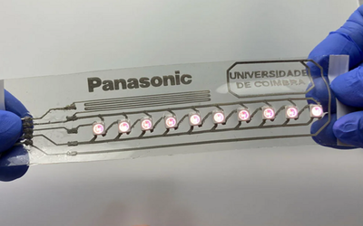
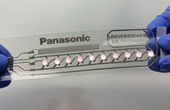
First-of-its-kind demonstration suggests a more environmentally friendly future for the electronics industry is possible
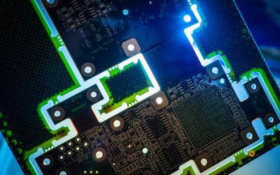
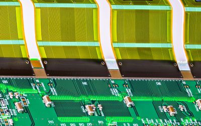
A novel stretchable film has been developed for soft & stretchable circuit / electronic solutions, outperforming existing films like TPU. Here you can learn about case studies showcasing its potential in pliable PCBs, stretchable hybrid PCBs, and truly stretchable electronics.
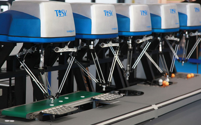
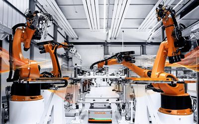
Find out the drivers and challenges that are facing the industrial robotics industry
Understanding the key differences between the two high-in-demand battery types. This article focuses on Energy density, lifespan, safety, and cost trade-offs for the technical selection of Li-Ion and LiFePO4 batteries.
16 minutes read.
20 minutes read.
15 minutes read.
20 minutes read.
13 minutes read.
28 minutes read.


Electronics
Mouser Electronics is a worldwide leading authorized distributor of semiconductors and electronic components.
219 Posts
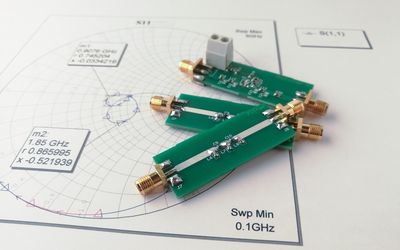
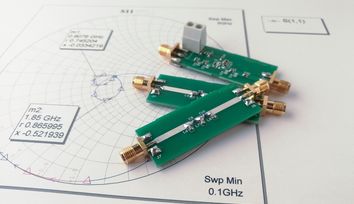
A guide covering the full radio-frequency design workflow, starting from setting specifications and choosing topologies to matching, simulation, layout, and verification, to help antenna engineers.
This article presents a detailed technical exploration of SiC MOSFET devices, covering material physics, device structure, switching behavior, and practical design considerations for high-efficiency power electronics systems.
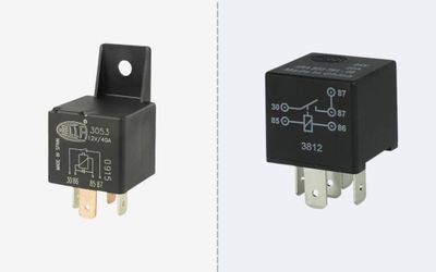
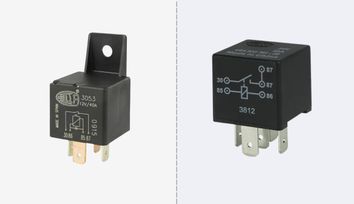
This article is a comprehensive technical guide to relay wiring diagrams, covering 4-pin and 5-pin configurations, working principles, safety practices, standards, and advanced relay applications in modern systems.
Explore how frequency shapes EMC behavior from RF emissions to ultra-low-frequency drift, with mitigation strategies for robust, compliant electronic system design.
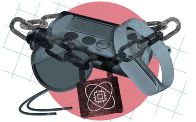
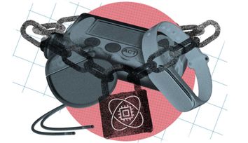
Ultra-efficient chip design enables extremely strong cryptography algorithms to run on energy-constrained edge devices.
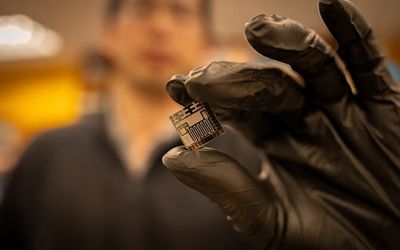
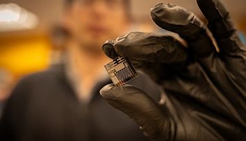
Researchers at ETH Zurich have now developed chip technology that enables verification of the authenticity of sensor data, including images or videos.
The integrated design achieves accurate micro gas chromatography and can help reduce the cost of monitoring chemical synthesis, natural gas pipelines or at-home air quality.
Hybrid bonding provides the adhesive free, copper to copper interconnects that are driving cutting edge 3D chip stacking. This article explains the theory, process, benefits, challenges, applications, and emerging trends of hybrid bonding for engineers.
First-of-its-kind demonstration suggests a more environmentally friendly future for the electronics industry is possible
A novel stretchable film has been developed for soft & stretchable circuit / electronic solutions, outperforming existing films like TPU. Here you can learn about case studies showcasing its potential in pliable PCBs, stretchable hybrid PCBs, and truly stretchable electronics.

3 minutes read
Find out the drivers and challenges that are facing the industrial robotics industry

3 minutes read
Castellated holes are extensively used in the printed circuit board (PCB) design process. This article is a detailed overview of castellated holes, covering their history, application, benefits, design attributes, challenges, and significance in modern electronic design.
SystemVerilog is the industry's leading hardware description and verification language (HDVL), offering a unified solution for digital system design and verification. This article delves into the fundamentals of SystemVerilog, highlighting its origins, key differences from Verilog, essential language elements, design constructs, and powerful verification features.
Delta arms are high-performance robotic arms that use parallel linkages and jointed construction to provide fast, precise, and flexible movement, making them ideal for various industrial and manufacturing applications.
Many companies are now looking at alternatives to silicon chips.
5 minutes read
Originally, the vast majority of GIS offered 2D displays, but with the advancement of technology, many systems now feature 3D displays capable of visualizing geospatial information more clearly for different purposes.

8 minutes read
This article offers an in-depth view of process control, including its history, fundamental concepts, components, strategies, and implementation in industrial systems.
Articulated robots are highly versatile and efficient robots that have the ability to mimic human arm movements for various industrial and commercial applications.
Electron beam evaporation is a physical vapor deposition process capable of applying nano-scale thin films to substrates.
Find out why rigid-flex PCB assembly has become increasingly popular in modern electronic production.
3 minutes read
Leaking fluids can wreak havoc if not detected at an early stage. This article showcases ultra-thin and flexible leak-detection solutions that can stick to any surface and immediately alert users in case of a leakage.
The IoT has been a game-changer for large-scale agricultural food growth. Through precision farming—which uses connectivity, sensors, machines, drones and data analytics—farmers can create the ideal crop growing conditions and achieve the best yield-to-input ratio.

3 minutes read
Thin film deposition is a process used to create thin film coatings on different materials. Thin films can consist of metal, semiconductors, and dielectrics, providing them with different properties. These properties translate to benefits such as electrical insulation, optical transmission, and corrosion resistance, that can be used to improve substrate performance. This article explores the processes of thin film deposition, along with its types, parameters, benefits, drawbacks, and applications.