Featured
Sensors are ubiquitous in our modern world, playing pivotal roles in numerous sectors. This article delves into their fundamental principles, diverse types, and their significant impact across industries.
Sensors are ubiquitous in our modern world, playing pivotal roles in numerous sectors. This article delves into their fundamental principles, diverse types, and their significant impact across industries.
PCB Trace Width Calculator
Glossary of Semiconductors Terms
Sensors are ubiquitous in our modern world, playing pivotal roles in numerous sectors. This article delves into their fundamental principles, diverse types, and their significant impact across industries.
Despite the prevalence of newer surface mount technology, THT still retains several unique benefits that underscore its enduring relevance. Find out which method is best for your projects.
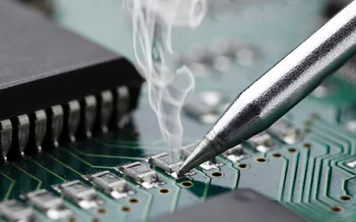
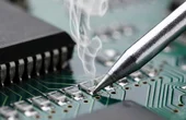
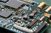
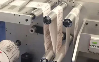
Castellation PCB is a type of printed circuit board (PCB) that has a series of small, plated through holes along the edges of the board. These holes are used to create a connection between the board and other components in a circuit. This article delves into the design, manufacturing, and testing processes involved in creating castellation PCBs, providing insights into the key considerations and guidelines that engineers and manufacturers should follow to optimize their designs for performance, reliability, and manufacturability.
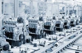
Semiconductors are the building blocks of modern electronics, powering everything from smartphones to satellites. This in-depth guide provides a comprehensive understanding of semiconductors' engineering principles and applications, delving into their fundamental concepts, materials, devices, manufacturing processes, and their impact on today's technology landscape.
13 minutes read.
20 minutes read.
16 minutes read.
20 minutes read.
20 minutes read.
13 minutes read.


Semiconductors
Nordic Semiconductor is a fabless semiconductor company specializing in wireless technology that powers the IoT.
181 Posts
A guide covering the full radio-frequency design workflow, starting from setting specifications and choosing topologies to matching, simulation, layout, and verification, to help antenna engineers.
This article presents a detailed technical exploration of SiC MOSFET devices, covering material physics, device structure, switching behavior, and practical design considerations for high-efficiency power electronics systems.
This article is a comprehensive technical guide to relay wiring diagrams, covering 4-pin and 5-pin configurations, working principles, safety practices, standards, and advanced relay applications in modern systems.
Explore how frequency shapes EMC behavior from RF emissions to ultra-low-frequency drift, with mitigation strategies for robust, compliant electronic system design.
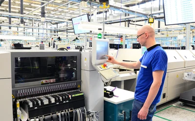
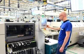
How Essentra Components Supports Engineering from Concept to Production
Makera gives live demonstrations of the Z1 during the 2026 Hackaday Europe event. The Z1 is a compact CNC manufacturing platform.
A crystal oscillator is an electronic circuit that uses a quartz crystal to produce a precise and stable frequency reference. This article covers crystal operation, equivalent circuit models, resonance, load capacitance, oscillator topologies, stability, aging, and design practices.
June 25, 2026 at 08:00 PM Central European Summer Time
Sensors are ubiquitous in our modern world, playing pivotal roles in numerous sectors. This article delves into their fundamental principles, diverse types, and their significant impact across industries.
Despite the prevalence of newer surface mount technology, THT still retains several unique benefits that underscore its enduring relevance. Find out which method is best for your projects.

10 minutes read
Castellation PCB is a type of printed circuit board (PCB) that has a series of small, plated through holes along the edges of the board. These holes are used to create a connection between the board and other components in a circuit. This article delves into the design, manufacturing, and testing processes involved in creating castellation PCBs, providing insights into the key considerations and guidelines that engineers and manufacturers should follow to optimize their designs for performance, reliability, and manufacturability.
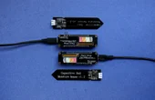
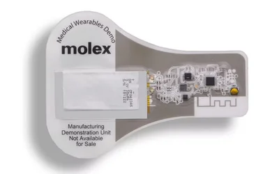
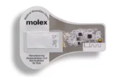
Status and evolution of intelligent skin patches, enabled by flexible hybrid electronics, going from a single wired sensors to complex wireless multi-function capability. Learn about trends, archirectures and challenges from a manufacturer's point of view to understand how to design for production.

4 minutes read
Article 3 of Bringing Intelligence to the Edge Series: Balancing the critical metrics of accuracy, power consumption, latency, and memory requirements is key to unlocking the potential of Tiny Machine Learning (TinyML) in low-power microcontrollers and edge computing.
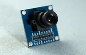
Article 2 of Bringing Intelligence to the Edge Series: Advancements in AI and embedded vision technologies are revolutionizing various industries, enabling real-time decision-making, enhancing security, and facilitating automation in various applications.
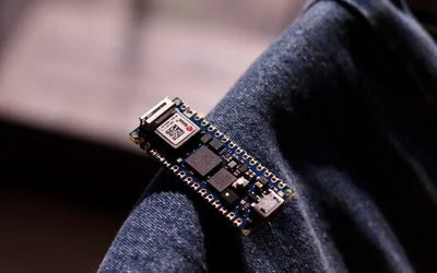
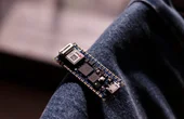
Article 1 of Bringing Intelligence to the Edge Series: With the introduction of AI, IoT devices can become more intelligent and less reliant on external systems— but not without trade-offs in performance and cost. Understanding how to make that decision is key.
Introducing the Bringing Intelligence to the Edge Series: Exploring how Artificial Intelligence is moving to embedded systems, transforming technology across various applications.
How IoT devices and SBCs improve the quality of life and care for elderly people
Semiconductors are the building blocks of modern electronics, powering everything from smartphones to satellites. This in-depth guide provides a comprehensive understanding of semiconductors' engineering principles and applications, delving into their fundamental concepts, materials, devices, manufacturing processes, and their impact on today's technology landscape.
The Inflation Reduction Act directs nearly $400 billion to clean energy incentives including $47 billion allocated for manufacturing. This article concentrates on the advantages offered to businesses.
5 minutes read
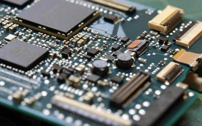
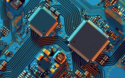
This article provides a detailed guide to System in Package technology, its advantages and challenges, key components, design, and manufacturing process.
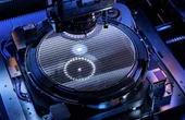
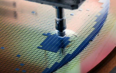
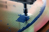
Wafer backgrinding is a crucial step in semiconductor manufacturing, as it prepares the wafer for further processing and packaging. The procedure comprises the thinning of silicon wafers by scraping out material from the backside, which is crucial for enhancing the functionality and dependability of semiconductor devices. This article examines the wafer backgrinding procedure, its difficulties, and the significance of quality control in ensuring the production of high-quality semiconductor devices.
Companies with strong ESG performance reduce costs by 5 to 10 percent.
7 minutes read
Healthcare is undergoing a transformative shift with the rise of stick-to-skin wearable monitoring devices. These data-collecting marvels, such as continuous glucose or cardiac monitoring devices, offer convenience & real-time insights.This article explores capabilities, applications & market trends
3 minutes read