Filled Vias: A Comprehensive Guide
Filled vias are via holes that are completely filled and closed with conductive or non-conductive material or copper plating. The filled via is one of the many realizations of PCB via covering, specified by industry standards. This article covers the definition, benefits, processes, applications, and challenges of filled vias.

09 Mar, 2023. 7 minutes read
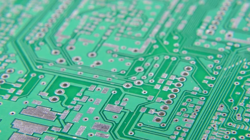
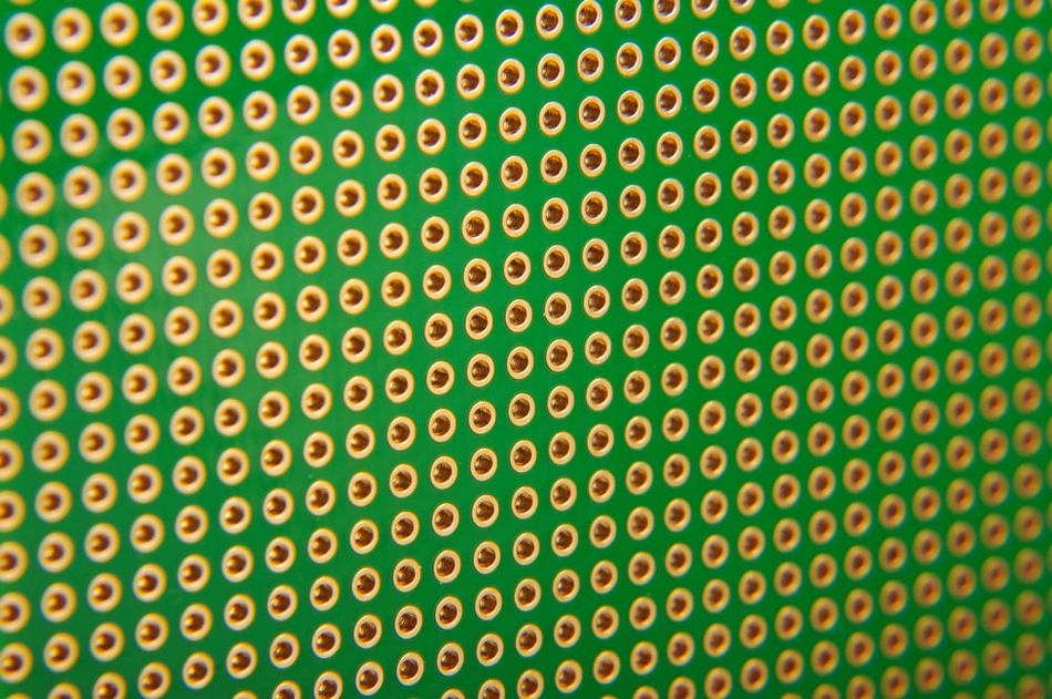
PCB with Via Holes
Introduction
A via is a metallic drilled hole that interconnects the circuitry of a circuit board. This hole transmits electrical signals between the various layers of a PCB. Therefore, it is especially useful for multilayer boards. Vias essentially serve as conductive pathways through which electrical signals travel between circuit layers. The advent of vias facilitated the production of smaller PCB sizes and more portable electronic devices, by implication.
Recommended Reading: What is a Via: A Comprehensive Guide
PCB manufacturers make the via hole conductive by placing copper cylinders in the drilled holes. Then they fill the inner layer of the via with a non-conductive material. There are different versions of via covering and filling, all specified in international standard IPC 4761. The Filled Via is one of these specifications. Via hole filling is a process where the via hole of a PCB is filled with a solder mask or resin.
Definition of Filled Via
A filled via is a via hole that is completely closed using a conductive or non-conductive epoxy material or copper plating. The practice of filling vias is a PCB manufacturing technique that serves to enhance the reliability of the circuit board by reducing the probable occurrence of trapped air or liquid in the via, which can lead to failures during the assembly process.
Benefits of using Filled Vias
Microvias, buried vias, and plated through-holes are filled with conductive or non-conductive materials for the following benefits:
Tighter BGA pitches
EMI reduction
Increased heat dissipation and electrical conductivity
Reduced layer count or board size, which translates to overall cost reduction
Boosts routing density
More secure Pad attachment
Gives high-frequency designs the shortest possible route to bypass capacitors
Negates problems in high-speed design and constraints such as low inductance[1]
Types of Filled Vias
There are options in the practice of filled vias, typed into the following:
Copper Filled Vias
To manufacture copper-filled vias, the PCB through holes are filled with epoxy resin and copper. This requires extra materials that hike the cost of board production, but copper-filled vias make a PCB more suitable for certain applications. They also possess capabilities that other conductive fillings do not offer.
PCBs with copper-filled vias are more beneficial than boards with copper-plated vias in the following aspects:
Thermal conductivity: When a via is filled with copper, its thermal conductivity increases. Keeping the heat away from the board will lengthen its lifespan and prevent defects in applications where high heat is required. Due to copper's strong thermal conductivity, this heat is drawn to it and kept off of the PCB's crucial sections. The heat flows through the copper from one side of the board to the other instead of moving to different parts of it.
Electrical conductivity: Copper-filled vias are also suitable for applications that involve the movement of strong currents from one side of the board to the other. Large currents can flow through to inner layers without overloading the PCB, due to the copper's conductivity. Due to this capability, designers frequently request copper-filled vias for PCBs that will be exposed to high voltage levels. Therefore, copper-filled vias are often preferred for PCBs that are made for high voltage levels.
Conductive Polymer Filled Vias
Conductive via filling improves the thermal transfer capabilities of the via while enabling efficient electrical signal transmission from one side of the circuit board to the other. The most common materials used in conductive filled vias are copper or silver epoxy. They do very well in conducting a large amount of heat away from components as the metallic nature of the fill transfers heat away from the IC to the other side of the board where it is further dissipated by a heat sink.
Although copper conductive epoxy has significantly superior heat conductivity, silver epoxy is more affordable and more often utilized. However, A conductive polymer layer deposition method on the via-hole of a printed circuit board can reduce manufacturing costs by directly metalizing the inner wall of the via hole without creating a void. All these will enhance the current flow between the vias and internal layers of the PCB.
It is noteworthy that there can be a significant difference in the coefficient of thermal expansion or CTE between the metallic fill and the surrounding laminate. Metal heats up and expands a lot faster than laminate. As a result of this uneven expansion, a fracture may develop between the pad and the hole wall.
Non-Conductive Filled Vias
Non-conductive filled vias are processed the same as conductive filled vias, however, instead of transferring heat and a signal, it is often done to stop solder or other impurities from entering the via. Moreover, it offers structural support for a copper pad that, in the case of a via-in-pad, covers the hole.
PCB manufacturers usually use the non-conductive epoxy paste to fill a regular via. The solder mask on these filled vias stops a few mils short of the pad. This is acceptable for medium-density boards because the presence of the solder mask lessens the possibility of solder bridging between the via and the nearby pad. The vias are still plated with copper, allowing them to carry heat and electrical signals. So the sole difference between these and traditional vias is that the fill material fills the gap in which air had existed.
It is always advised to match the CTE values of the via filling to be applied with the surrounding laminate to avoid future stress fractures brought on by expansion or contraction from the same circumstances as previously described in conductive filled vias. [2]
Filled Vias Manufacturing Process
The manufacturing process for filled vias, just as in general PCB fabrication, requires the board to be cleaned and prepped. After ensuring that it is devoid of contaminants, the via-filling process can begin.
Drilling of Vias
Two common methods for creating vias are the use of mechanical drill bits, and the use of a laser beam (usually used for microvias). All these methods have their own advantages and drawbacks. The choice of the method is made considering various factors like cost, number of PCBs in production, the required precision, hole depth, diameter, etc.
To avoid breakout during drilling, the annular ring around the hole where the vias are installed must be sufficient. This risk is present because mechanical drills tend to stray a little bit during the fabrication process. Via drill sizes must also be calculated with the proper aspect ratio, for an effective drill to be achieved.
Cleaning of Vias
The via holes are cleaned of debris from the drilling operation. This can range from burrs on the edge of the holes to resin residue inside the holes. Cleaning is done using a combination of abrasive mechanical and chemical processes.
Moreover, cleaning the PCB with a brush and solvent ensures a finer and smoother drilling process. The board goes through numerous baths for cleaning and plating, and the entire process is closely monitored to ensure that copper is evenly plated within the via holes.
Filling of Vias
In this stage, the via is filled with non-conductive or conductive material. The process of filling the holes with resin is conducted in two phases. In the first, the holes are filled with pressure and vacuum to allow efficient filling of the holes without developing gaps in the resin. Then in the second phase, a surface cleaning of the panel is conducted to get rid of the excess resin. This serves as a prep for the following planarization.
Planarization of Filled Vias
After polymerization is complete, the resin is removed by a mechanical brushing action, called planarization, which is typically performed with specialized machines that employ cup brushes or with horizontal brushing machines. This process essentially involves flattening and smoothening the copper surface, aimed at removing the excess resin and creating a uniform surface. It prepares the filled vias for over-plating with copper to allow the ideal soldering of electronic components. [3]
Applications of Filled Vias
Filled vias are instrumental in the implementation of Via-In-Pad. In this process, vias are filled, planarized, and plated over with copper. It is also known as active pad and is gaining popularity and increased preference to transmit signal from the BGA through the via and onto inner layers instead of the traditional “dog bone” method. The Via-In-Pad process can have major advantages over through-hole technology, even though it is cost intensive. Moreover, filled vias are highly applicable for PCBs of medium density as the solder mask minimizes the chances of solder bridging between the pad and the via.
Challenges in using Filled Vias
Filled vias offer many benefits for PCB fabrication, however, manufacturers face some challenges in implementing them with different applications. As a prominent product of filled vias, Via-in-pads show some fabrication issues. For instance, the soldering process can cause the via hole to get filled up, making it useless. Therefore, a minimal number of via-in-pads is recommended.
Also, the copious intermediate steps required make filled vias cost-intensive and there is the present risk of uneven copper erosion during resurfacing, as well as structuring-related issues. [4]
Key Takeaways
The filled via is the result of a PCB manufacturing technique that involves filling a via hole with epoxy to completely close the hole. The epoxy filling can be done with a conductive or non-conductive material, thereby creating distinct types of filled vias. Filled vias facilitate more reliable surface mounts (SMD), better assembly yields, and improved PCB reliability.
References
1. PCB Directory. What is Via Filling? 2021. [Cited 2023 Mar 6] Available from: https://www.pcbdirectory.com/community/what-is-via-filling
2. Moko Technology. What is PCB Via?. 2022. [Cited 2023 Mar 6] Available from: https://www.google.com/amp/s/www.mokotechnology.com/what-is-pcb-via/amp/
3. PCB Universe. Via Tenting, Plugging, and Filling. 2022. [Cited 2023 Mar 6] Available from: https://www.pcbuniverse.com/pcbu-tech-tips.php?a=5
4. NCAB Group. Via Hole Plugging - What is it and When Can it be Used? 2021. [Cited 2023 Mar 6] Available from: https://www.ncabgroup.com/blog/via-hole-plugging-what-is-it-and-when-can-it-be-used/