Mastering PCB Testing: Techniques, Methods, and Best Practices Unveiled
Testing PCBs involves using various methods and tools to ensure that all the individual elements of a PCB perform optimally, making up a high-quality PCB assembly. This article delves into the methods, procedures, and requirements of PCB testing.

Last updated on 01 Mar, 2024. 21 minutes read
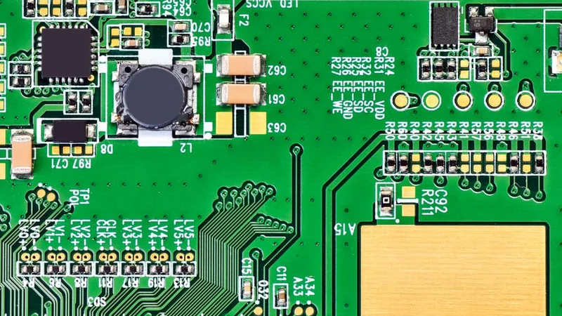
Electronic Circuit Board
Introduction to PCB Testing
Testing is integral to PCB manufacturing, ideally conducted throughout the production cycle to avoid errors in the final product. Early application of PCB design analysis techniques can minimize major issues during manufacturing. Various testing methods on physical boards, including prototypes and small-scale assemblies, focus on potential shorts, solder joint issues, and functionality, ensuring each PCB functions correctly. Hence maintaining the reliability and performance of electronic products.
Without thorough testing, faulty PCBs could lead to product failures, which can have significant consequences, including financial losses and damage to a company's reputation. PCB testing is a complex process that requires specialized equipment and expertise. It involves a variety of tests, each designed to check a specific aspect of the PCB's functionality. These tests range from simple visual inspections to more complex electrical tests that check the PCB's performance under different operating conditions.
In the rapidly evolving world of electronics, PCB testing continues to play a vital role. As electronic devices become more complex and integrated, thorough and accurate PCB testing becomes even more critical. By ensuring the quality and reliability of PCBs, testing helps drive the advancement of electronic technology and contributes to the creation of high-quality, reliable products.[1]
The Importance of PCB Testing
PCB testing plays a pivotal role in the electronics industry, primarily because it is instrumental in ensuring the quality and reliability of electronic products. PCB testing involves thoroughly examining the PCBs to detect potential issues or defects that could compromise the final product's functionality.
The consequences of inadequate PCB testing can be severe. For instance, a faulty PCB can lead to the failure of an electronic device, which can have significant implications. From a financial perspective, product failures can result in costly recalls, repairs, and replacements. Moreover, these failures can also lead to a loss of customer trust, harming a company's reputation and market position.
In the context of safety-critical applications, such as medical devices or automotive electronics, the importance of PCB testing is even more pronounced. A malfunctioning PCB in these applications could potentially lead to safety risks, making rigorous testing essential.
Furthermore, PCB testing is also crucial from a regulatory compliance perspective. Many industries have stringent standards and regulations related to the quality and performance of electronic products. PCB testing helps ensure these standards are met, facilitating regulatory compliance.
In essence, PCB testing is a critical quality assurance measure that helps mitigate risks, ensure regulatory compliance, and uphold the reliability and performance of electronic products. It is a non-negotiable aspect of the electronics manufacturing process, underpinning the delivery of high-quality, reliable, and safe electronic devices.[2]
How Do You Test a PCB Board?
A PCB comprises different elements affecting the electronic circuit's overall performance. Tests are carried out to check and optimize the status of these elements using computerized machine software, simple electronic testing equipment and tools, and even basic human inspection. These checks include but are not limited to the following:
Electrical tests, which also include measuring leakage currents
Quality of hole wall
Mechanical resistance test
Quality of the welds
Copper plating was tested with tensile strength, and the following stretching was analyzed.
Cleanliness checks, accounting for weather resistance, humidity, and corrosion
Component alignment, polarity, placement, and orientation
Lamination, which tests the laminate's resistance to peeling by force or application of heat
Environmental tests are particularly necessary for PCBs used in humid environments. [3]
Further reading: PCBA vs PCB: The foundation of modern-day electronics
Types of PCB Tests
PCB testing employs various test types, each assessing specific aspects of the PCB's functionality. These tests are integral to the process, comprehensively evaluating the PCB's performance and reliability.
Common PCB tests include the In-Circuit Test (ICT), which checks component functionality by applying current and measuring resulting voltage, useful for detecting issues like short circuits and incorrect values. The Functional Test verifies overall functionality by powering up and running the PCB through operations. The Flying Probe Test uses probes to test electrical properties without custom fixtures, which is ideal for small PCB batches. PCBs can be tested by engaging the following testing methods:
In-Circuit Testing
In-circuit testing (ICT) is the most potent type of PCB testing available. It is also known as a "bed-of-nails test," used to verify that each electronic component on the PCB is in its proper location and is operating properly. Short circuits, open circuits, resistance, capacitance, and other factors are checked throughout the test.
Fixed probes arranged following the PCB's layout are used for this test. The probes examine the solder connection's integrity. To begin the test, the bed of nails tester presses the board against the bed of probes. The board has access points already constructed to connect the ICT testing probes to the circuit. They exert a certain amount of pressure on the connection to ensure it is secured. The ICT is usually performed on bigger connections and ball grid arrays (BGAs).
The bed-of-nails technique is expensive and needs to be more adaptable since each board requires its bed-of-nails. Also, it demonstrates some challenges in testing boards with high component density, where pin spacing is decreased. The ICT method offers the advantage of identifying flaws in the individual components and their connections without powering the board. Its drawbacks include the high cost, exacerbated by the complexity of the bed of nails and the control software. Another demerit is the inability to test the connectors. [4]
Flying Probe Testing
The Flying probe test, also known as the fixtureless in-circuit test (FICT), is a type of in-circuit test that operates without specialized test fixtures, lowering the overall cost. With this technique, a basic fixture holds the board in place while a software-controlled program moves test pins about and checks specific test points. Due to its versatility, the flying probe test is well-liked throughout the electronics manufacturing industry.
Although flying probe testing is used for the same purposes as conventional ICT, it has significant benefits and drawbacks because of how it is conducted. While the flying probe can rapidly, efficiently, and affordably adapt to different boards with a simple programming change, it is typically slower than the conventional ICT. This characteristic makes it a perfect testing technique for prototype and small-production tests but less efficient for large-scale production. [5]
Automated Optical Inspection (AOl)
AOI is a visual inspection for printed circuit boards that require no contact. Cameras and microscopes are used in AOI to take pictures of the PCB. The software then looks for inconsistencies between these photos and the board's schematic. Technicians may thoroughly inspect each board and spot any issues by this procedure. The board is not powered up during AOI and may not cover all part types. Due to these inadequacies, it should be combined with another test technique, such as functional testing, flying probe testing, or ICT.
A PCB's performance can be impacted by various faults that AOI can detect. It can specifically find solder gaps, excess solder, and under- and over-etching. It also covers component defects, such as those that are missing and have the wrong values and components positioned or aligned incorrectly. Moreover, AOI can recognize and rectify BGA shorts and open circuit connections and detect lifted lead deficiencies on PCBs.
AOI can be performed at any stage of the manufacturing process. It can be placed right before, during, or after reflow soldering, where most errors occur. This way, any discovered issues can be immediately corrected, ensuring more products pass the final inspection or board testing methods. [6]
Further reading: What is AOI (Automated Optical Inspection): A Comprehensive Guide
Burn-In Testing
Burn-in testing is an intensive type designed to analyze PCBs' load capacity and detect early errors. The printed circuit boards go through electrical or thermal testing during this process. In the first instance, electricity is continually applied to the board for about 40 to 160 hours. Another option to examine the PCBs' performance at high temperatures is to expose them to temperatures up to 125 degrees Celsius for 160 hours or longer. The printed circuit boards may frequently also be put through an environmental stress test. Infant mortality is the term used when a board fails.
The ICs are mounted on the board and under stress while being tested. The board utilized for the burn-in test is constructed from FR4 flame retardant material, which enables it to endure temperatures of up to 125 degrees Celsius. Boards of ceramic and polyamide are applied when the board's temperature exceeds 125 degrees Celsius. The boards are tested in the burn-in oven using the required voltage. The board is removed when the stress test is finished and examined for flaws. Sockets are provided to hold the ICs on the boards.
It is important to note that burn-in testing can reduce the lifespan of the circuit board, particularly if the test subjects the board to greater stress than it is designed to withstand. To prevent overstressing the PCB, the testing limit may be lowered after a shorter time if few or no flaws are discovered. [7]
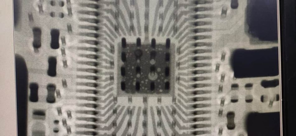
X-Ray Inspection
As the name implies, this type of testing is essentially an inspection tool. It is also referred to as AXI. During this test, an X-ray technician can find flaws early in the production process by scrutinizing solder connections, internal traces, and barrels. Inspectingnspect components out of sight using X-ray inspection, like connectors and ball grid array packages with solder joints under the chip p, is possible. This check typically requires skilled, knowledgeable operators.
More precise inspection techniques, such as those based on X-ray technology, were necessary due to the high density provided by SMT technology and the difficulties in locating connections in BGA and CSP (Chip Scale Packages). Welds can be seen clearly in radiographic pictures because they are formed of a material having a higher atomic weight than the other components on the board.
The primary benefit of the AXI technique is that it can identify every connection and weld, including those concealed by the package. Additionally, solder joints can be examined, highlighting any potential bubbles. There is also a good chance of finding any exclusive electronic components replicas. However, this technique is known to be a time-consuming and expensive process. [8]
Stress Test
Stress Test in PCB testing is a crucial method used to determine the reliability and robustness of a printed circuit board under various conditions. This type of testing evaluates a circuit board's ability to withstand or endure forces or strains that may be placed on it during operation.
Stress tests are designed to simulate extreme conditions that the PCB might encounter during its lifetime, such as high temperatures, high voltages, mechanical stress, and environmental factors like humidity or vibration. By subjecting the PCB to these conditions, engineers can assess its performance and reliability under stress, ensuring that it meets the required standards and specifications.
During a stress test, the PCB is typically exposed to these conditions for a specified period while its performance is monitored. The test may involve applying a higher-than-normal voltage to the PCB, exposing it to elevated temperatures, or subjecting it to mechanical vibrations. The goal is to identify any weaknesses or potential points of failure in the PCB's design or components.
The results of a stress test can provide valuable insights into the PCB's reliability and durability. They can help identify areas where the design or components need improvement to ensure the PCB can perform reliably under real-world conditions. Stress testing is especially important for critical applications where the failure of a PCB could have serious consequences, such as in aerospace, automotive, or medical devices.
Design for Testing (DFT)
Design for Testing (DFT) is not a PCB test method per se but rather a design approach used to facilitate testing during the PCB manufacturing process. DFT involves designing the PCB to make testing its functionality and quality easier and more efficient.
One of the key aspects of DFT is the inclusion of testability features in the PCB design. These features can include built-in test points, access points for probes, and test circuits that allow easy and accurate testing of the PCB's functionality. Manufacturers can reduce the time and cost of testing and troubleshooting by designing the PCB with these features.
DFT also involves considering testability throughout the entire design process. This means ensuring that the PCB layout and component placement are optimized for testing and that the design includes features that make it easier to diagnose and correct any issues that may arise during testing.
Overall, DFT is an important aspect of PCB design that can help ensure the quality and reliability of the final product. By designing PCBs with testability in mind, manufacturers can improve the efficiency of the testing process and reduce the likelihood of defects in the finished product.
Functional Testing
Functional testing, as its name suggests, is aimed at testing a circuit's functionality by simulating the electrical signals capable of stimulating it and observing the results. It is the final stage of PCB inspection and verification. Through the interface connectors, the circuit is accurately powered and electrically stimulated. A software program analyzes the measurements taken at appropriate locations on the PCB and confirms that they match the design requirements.
The functional testing process ensures that the final product works as it should. This test could be as simple as an on/off power test or as in-depth as a test using testing software. The ultimate goal of the testing process is to pinpoint and rectify any issues that may arise after a product has been completed. The procedure tests the board's digital and analog signals to simulate operation. It may also employ specialized software to detect circuitry issues. Manual inspections of various aspects of the PCB manufacturing process may also be included.
The functional test can detect potential circuit anomalies that only appear when the circuit is powered. In addition, it can measure the power absorption at particular circuit points. The expense and complexity of the test system are the drawbacks. It requires equipment that is extremely complex but not very adaptable, as it is frequently configured just to examine a single card.
Other Functional Tests
Other functional tests can be used to examine a PCB, depending on the situation. A PCB functional test confirms how a PCB behaves in the product's application environment. Depending on the PCB and final product, the requirements for a functional test and its development and methods can differ significantly.
Other functional tests for PCB assembly include:
Solderability Test: This is done to check whether a component offers the wetting required for a strong solder connection. A subpar test result suggests a subpar connection. Before completing assembly, it is crucial to do solderability testing, which is an essential component of PCB functional testing. When the metal doesn't solder during the test, it reveals that the PCB has flaws that will impair its performance. As a result, the PCB could experience solder oxidation and other undesirable issues.
Contamination Testing: Detects ionic residues from manufacturing and soldering processes. It is necessary to ensure ionic cleanliness before applying the conformal coating to printed circuit boards. Contamination testing also successfully removes most non-ionic contaminants that can degrade the board, causing corrosion and other problems.
Micro-Sectioning Analysis: This tool is effective for failure analysis and in-process verification. It is a threefold inspection tool for checking the internal makeup of a PCB for defects, opens, shorts, and other failures. Typically, the inspection criteria for the Micro-Section Analysis are included in the product specification designated by the customer. The analysis could, however, also adhere to guidelines like IPC 6012, MIL-PRF55110/31032, or both.
Time-Domain Reflectometer (TDR): A time-domain reflectometer is a tool to locate problems in transmission lines and coaxial cables. The TDR scans the transmission line with a low-voltage pulsed signal to look for any reflections caused by an impedance mismatch.
There won't be any reflections if there is no impedance mismatch over the transmission line. However, if there is a break in the transmission line at a specific location, a portion of the pulsed signal will be reflected to the TDR. The TDR can determine the precise position of the fault and the type of fault, such as an open circuit, short circuit, or impedance mismatch, by calculating the timing and propagation velocity of the received pulse.
Peel Testing: is the practice of testing adhesion properties of film bonded to the substrate, usually by tensile. This is done to determine the strength required to peel the laminate from the board.
Solder Float Testing: Determines the thermal stress a PCB's holes can withstand. To carry out this test, extreme temperatures are applied while measuring the resistance of the PCB's holes. [9]
Further reading: Demystifying Soldering Techniques: A Comparison of Wave Soldering and Reflow Soldering
PCB Testing Equipment
The effectiveness of PCB testing relies heavily on the quality and appropriateness of the testing equipment. The choice of equipment can vary based on the test type, PCB complexity, and testing volume.
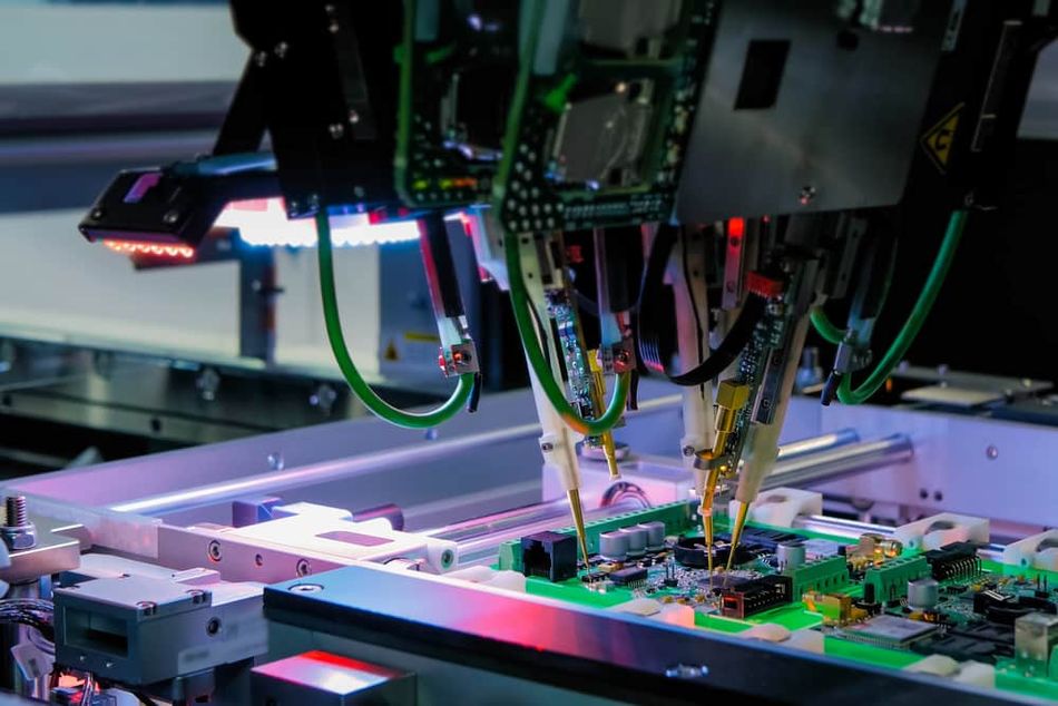
One commonly used device is the bed of nails tester, which features spring-loaded pogo pins that make contact with the PCB, enabling current application and voltage measurement to assess component functionality. This tester is mainly used for In-Circuit Tests (ICTs) and requires custom fixtures for each PCB design. Another popular piece of equipment is the flying probe tester, utilizing movable probes for testing without requiring custom fixtures, making it adaptable to various PCB designs, ideal for small batches or prototypes.
Automated Test Equipment (ATE) is also prevalent, offering quick and accurate testing for high-volume production. ATE combines hardware and software that are programmable to conduct various tests, from basic electrical to complex functional tests. Below are the full details about these types of equipment used in PCB testing:
Test Fixtures
Test fixtures are a critical component of many PCB testing processes. They are custom-made devices that hold the PCB in place during testing and provide a means for the testing equipment to interface with the PCB.
In the context of a bed of nails tester, the test fixture includes a custom array of pogo pins corresponding to the PCB test points. The fixture ensures that each pin makes reliable contact with its corresponding test point, allowing the tester to apply a current to the PCB and measure the resulting voltage.
Test fixtures are typically designed and manufactured based on the specific requirements of the PCB design. This includes the layout of the components on the PCB, the location of the test points, and the electrical specifications of the PCB. The design and manufacture of test fixtures require a high degree of precision to ensure accurate and reliable testing.
While test fixtures provide a robust and reliable means of testing PCBs, they also have limitations. They can be time-consuming and costly to produce, particularly for complex PCB designs. Furthermore, any changes to the PCB design may require modifications to the fixture or the production of a new fixture. This is one of the reasons why alternative testing methods, such as the flying probe test, are often used for prototypes and small production runs.
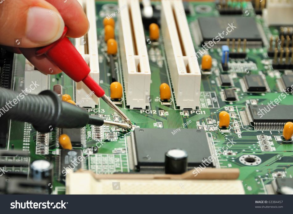
Test Probes
Test probes are essential tools in PCB testing, serving as the physical interface between the test equipment and the PCB. They are designed to make reliable, repeatable contact with the test points on the PCB, allowing the test equipment to apply signals to the PCB and measure the responses.
In a bed of nail testers, the test probes are typically spring-loaded pogo pins arranged in a custom fixture to match the test points on the PCB. These pogo pins are designed to make reliable contact with the PCB, even if the surface of the PCB is slightly uneven or the alignment is not perfect. The spring-loaded design ensures consistent pressure against the PCB, providing a reliable electrical connection.
Pogo pins come in various sizes and shapes to accommodate different test points and PCB designs. For instance, some pogo pins have a pointed tip for piercing through the protective coating on a PCB, while others have a flat tip for making contact with exposed pads or vias. The choice of pogo pin can significantly impact the reliability and accuracy of the test results.
In a flying probe tester, the test probes are attached to precise, motor-driven arms that can move quickly and accurately to different test points on the PCB. These probes can be programmed to touch down on specific points on the PCB, applying signals and measuring responses. The flexibility of the flying probe tester allows it to adapt to different PCB designs without the need for custom fixtures.
Regardless of the type of tester, the quality and design of the test probes are critical factors in the accuracy and reliability of the PCB testing process. They must be designed to make reliable contact with the PCB, withstand repeated use, and provide accurate and consistent measurements.
Automated Test Equipment (ATE)
Automated Test Equipment (ATE) is a significant component in the PCB testing process, particularly in high-volume production environments. ATE systems are designed to perform tests quickly and accurately, reducing the time and cost associated with manual testing.
ATE systems typically consist of a combination of hardware and software. The hardware includes the test probes and fixtures that interface with the PCB and the instruments that generate signals and measure responses. The software controls the operation of the hardware, directing the sequence of tests and analyzing the results.
One of the key advantages of ATE is its speed. ATE systems can perform a series of tests in seconds, making them much faster than manual testing methods. This speed is particularly beneficial in high-volume production environments, where hundreds or thousands of PCBs must be tested daily.
Another advantage of ATE is its accuracy. ATE systems are designed to provide precise, repeatable measurements, reducing the risk of human error that can occur with manual testing. This accuracy is critical for detecting subtle defects that might otherwise go unnoticed.
ATE systems can also be programmed to perform various tests, from simple electrical to more complex functional tests. This flexibility allows the ATE system to adapt to different PCB designs and testing requirements.
Despite these advantages, ATE systems can be expensive to purchase and maintain, requiring high technical expertise to operate and program. However, for many manufacturers, speed, accuracy, and flexibility benefits outweigh these costs.[10]
PCB Testing Procedures
PCB testing procedures are structured steps that guide testing printed circuit boards to ensure they meet the required specifications and function correctly in their intended application. These procedures are critical to the manufacturing process, as they help to identify defects or issues that could lead to product failure.
The general procedures for PCB testing typically begin with a visual inspection to identify any obvious physical defects, such as cracks, scratches, or misaligned components. Following this, electrical tests are conducted to verify that the PCB operates according to design specifications. These tests can include In-Circuit Testing (ICT), Functional Testing, and Flying Probe Testing, among others.
Each test has specific procedures that must be followed to ensure accurate and reliable results. For example, ICT requires setting up a bed of nail testers with custom fixtures to contact test points on the PCB. At the same time, Functional Testing involves simulating the operating environment of the PCB to test its performance.
The procedures also include calibrating and maintaining testing equipment to prevent inaccuracies. Regular calibration ensures that the equipment is providing correct measurements, which is essential for maintaining the integrity of the testing process.
After testing, the results are analyzed to determine if the PCB passes or fails the tests. If a PCB fails, it may undergo rework or be discarded, depending on the nature of the defect. The testing procedures help ensure that only PCBs that meet the required standards move on to the next production stage or are shipped to customers.
Test Planning
Test planning is a critical phase in the PCB testing process, laying the groundwork for a successful and efficient testing operation. A well-structured test plan outlines the objectives, scope, methodology, and resources required for testing, ensuring that all aspects of the PCB are thoroughly evaluated.
The key elements of a test plan include defining the tests to be performed, such as ICT, Functional Testing, or Flying Probe Testing, and determining the sequence in which they will be conducted. The plan should also specify each test's testing criteria and pass/fail thresholds. Another important aspect of test planning is the selection of appropriate testing equipment and fixtures. This involves choosing equipment capable of performing the required tests with precision and reliability.
Resource allocation is also a part of test planning. This includes assigning qualified personnel to conduct the tests and ensuring the testing schedule aligns with production timelines. Adequate training for the testing team is essential to ensure they are familiar with the testing procedures and equipment. Finally, the test plan should include provisions for data collection and analysis. This involves setting up systems to record and analyze test results to identify trends or recurring issues. The analysis can provide insights into the manufacturing process and help identify areas for improvement.
Test Analysis
Test analysis in PCB testing involves several analyses to ensure the functionality and reliability of printed circuit boards (PCBs). Some common types of test analysis include:
Failure analysis involves investigating and determining the root cause of failures or defects detected during testing. It helps in understanding why a PCB failed and how to prevent similar issues in the future.
Statistical analysis: Statistical methods are used to analyze test data to identify trends, patterns, or anomalies. This analysis can help improve the testing process and identify areas for optimization.
Correlation analysis: This analysis examines the relationship between different variables in the testing process to determine if changes in one variable affect another. It helps in understanding the impact of different factors on test results.
Trend analysis: Trend analysis involves tracking changes in test results over time to identify patterns or deviations from expected behavior. It helps predict future performance and identify potential issues early on.
Root cause analysis (RCA): RCA is a systematic process for identifying the underlying cause of a problem. It involves analyzing data and test results to determine what caused a specific issue or failure.
Comparative analysis: This involves comparing the performance of different PCBs or different batches of PCBs to identify variations or discrepancies. It helps in ensuring consistency and quality across different production runs.
Data mining: Data mining techniques extract useful information from large datasets generated during testing. It helps uncover hidden patterns or relationships in the data that can provide valuable insights for improving the testing process.
These test analyses are essential for ensuring PCBs' quality, reliability, and performance, ultimately leading to better products and customer satisfaction.
PCB Testing and Test Analysis
PCB testing and test analysis are closely related but distinct processes in the world of electronics manufacturing:
Similarities:
Both are essential to the PCB manufacturing process, ensuring the final product meets quality and functionality standards.
They involve using various methods and techniques to assess the performance and reliability of PCBs.
Both aim to identify and rectify any issues or defects in the PCB to ensure its proper functioning.
Differences:
PCB testing focuses on physically testing the PCB through methods like In-Circuit Testing (ICT), Flying Probe Test, and Functional Testing (FCT). It involves applying stimuli to the board and measuring its responses to validate its performance.
Test analysis, on the other hand, involves the interpretation of test results to diagnose and understand the root causes of any failures or anomalies detected during testing. It aims to provide insights for process improvement and quality enhancement.
PCB testing is more hands-on and practical, involving direct interaction with the PCB. At the same time, test analysis is more analytical and strategic, involving data interpretation and decision-making based on test results.
PCB testing is typically conducted by technicians and engineers on the production floor, while test analysis may involve specialized teams or individuals with expertise in data analysis and problem-solving.
In summary, PCB testing is the physical evaluation of the PCB. At the same time, test analysis is interpreting and evaluating the test results to improve the manufacturing process and product quality.
Challenges in PCB Testing
PCB testing is essential but faces several challenges:
Increasing Complexity: PCB designs are becoming more intricate, with higher component densities and smaller form factors, making it harder to access test points and increasing the risk of undetected defects.
Cost: High-end testing equipment like ATE and X-ray inspection systems can be expensive to purchase and maintain. Testing can also increase production costs, especially if rework is needed due to test failures.
Speed: Setting up and programming ATE systems can be time-consuming, creating bottlenecks in high-volume production environments, particularly with multiple PCB designs.
Accuracy: Despite being designed for precision, testing equipment can still have errors due to calibration issues, software bugs, or human error.
Keeping Up with Technology: As new components and technologies emerge, testing procedures and equipment need frequent updates, requiring ongoing investment in equipment and training to stay current.
Conclusion
PCB testing is an essential phase in the lifecycle of electronic product development. It ensures that the PCBs, which form the backbone of all electronic devices, function correctly and meet the required quality standards. The testing process encompasses various methods designed to uncover potential issues, from physical defects to functional anomalies. The complexity of modern PCBs, with their high component densities and advanced technologies, necessitates a comprehensive approach to testing. This ensures that the products that rely on these PCBs are reliable, safe, and perform as expected. The challenges faced in PCB testing, such as the increasing complexity of designs and the cost of testing, are significant but can be mitigated through careful planning, appropriate testing methods, and ongoing investment in technology and training.
Frequently Asked Questions (FAQs)
What is PCB testing, and why is it important? PCB testing checks the functionality and quality of printed circuit boards before they are used in electronic devices. It is important because it helps prevent defects that could lead to product failures, ensuring reliability and safety.
What are some common PCB testing methods? Common PCB testing methods include In-Circuit Testing (ICT), Functional Testing, Flying Probe Testing, Automated Optical Inspection (AOI), and X-ray inspection. Each method targets different potential issues and is chosen based on the specific needs of the PCB.
How does PCB complexity affect testing? Testing becomes more challenging as PCBs become more complex, with smaller components and higher densities. Access to test points is more difficult, and defects will likely go undetected. This requires more advanced testing techniques and equipment.
What are the challenges in PCB testing? Challenges in PCB testing include the increasing complexity of PCB designs, the high cost of testing equipment, the need for speed in high-volume production environments, the accuracy of testing, and keeping up with evolving technology.
Can PCB testing be automated? Yes, PCB testing can be automated, especially in high-volume production settings. Automated Test Equipment (ATE) can perform a series of tests quickly and accurately, reducing the time and cost associated with manual testing.
What factors influence the cost of PCB testing? Factors influencing the cost of PCB testing include the complexity of the PCB design, the type of tests required, the volume of PCBs being tested, and the cost of the testing equipment and maintenance.
Reference
WellPCB, n/a. PCB Testing Ultimate Guide To Prototype & PCB Assembly Testing. Available at: https://www.wellpcb.com/pcb-testing.html
Clarydon, n/a. The Importance of PCB Testing. https://www.clarydon.com/importance-pcb-testing#:~:text=The%20testing%20phase%20of%20PCB,and%20defects%20in%20the%20field.
Seed Studio. 7 Most Popular PCB Testing Methods During Manufacturing and Assembly. 2021. [Cited 2023 Feb 16] Available from: https://www.seeedstudio.com/blog/2021/06/18/7-most-popular-pcb-testing-methods-during-manufacturing-and-assembly/
ConRo Electronics. What is In-Circuit Testing (ICT)? 2022. [Cited 2023 Feb 16] Available from: https://www.conro.com/what-is-in-circuit-testing-ict/
Candor Industries. Flying Probes and Testing: Everything You Need to Know. 2021. [Cited 2023 Feb 16] Available from: https://www.candorind.com/flying-probes-and-testing-everything-you-need-to-know/
Valley Services Electronics. Using Automated Optical Inspection (AOI) for PCB Manufacturing Validation. 2021. [Cited 2023 Feb 17] Available from: https://www.vse.com/blog/2021/02/11/using-automated-optical-inspection-aoi-for-pcb-manufacturing-validation/
EMS Solutions. Importance of Burn-In Testing for PCBs. 2022. [Cited 2023 Feb 17] Available from: https://www.myemssolutions.com/importance-of-burn-in-testing-for-pcbs/
Electronics and You. 6 Benefits of PCB X-Ray Quality Control and Inspection. 2022. [Cited 2023 Feb 17] Available from: https://www.electronicsandyou.com/benefits-of-x-ray-inspection-of-pcb-for-quality-control.html
Seed Studio. Everything You Need to Know about PCB Assembly Functional Testing. 2021. [Cited 2023 Feb 17] Available from: https://www.seeedstudio.com/blog/2021/06/18/pcba-functional-testing/
Brett Daniel, 2021. What Is Automatic Test Equipment (ATE)? [Cited 2023 Feb 17] Available from: https://www.trentonsystems.com/en-us/resource-hub/blog/automatic-test-equipment-overview
in this article
1. Introduction to PCB Testing2. The Importance of PCB Testing3. How Do You Test a PCB Board?4. Types of PCB Tests5. PCB Testing Equipment6. PCB Testing Procedures7. PCB Testing and Test Analysis8. Challenges in PCB Testing9. Conclusion10. Frequently Asked Questions (FAQs)11. Reference