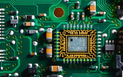
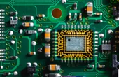
Semiconductors

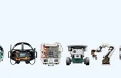
What’s Next for Artificial Intelligence and Edge Computing?
PCB Trace Width Calculator
Glossary of Semiconductors Terms


Engineers Wiki. Most Asked Questions.

Semiconductors are the building blocks of modern electronics, powering everything from smartphones to satellites. This in-depth guide provides a comprehensive understanding of semiconductors' engineering principles and applications, delving into their fundamental concepts, materials, devices, manufacturing processes, and their impact on today's technology landscape.
GaN HEMT: Gallium Nitride Power Transistors
13 minutes read.
What is VHDL? A Complete Guide with Syntax, Examples & IEEE Standards
20 minutes read.
DC Motor Speed Control: PWM Techniques for Brushed and BLDC Drives
16 minutes read.
Crystal Oscillator: Fundamentals, Models, and Design Guidelines
20 minutes read.
Bandgap Voltage Reference: Complete Guide for Analog Engineers
20 minutes read.
How to Charge a Lithium-Ion Battery Safely and Efficiently?
13 minutes read.
ORGANIZATIONS. SHAPING THE INDUSTRY.


Nordic Semiconductor
Semiconductors
Nordic Semiconductor is a fabless semiconductor company specializing in wireless technology that powers the IoT.
181 Posts


TAGGED WITH flexible electronics

A guide covering the full radio-frequency design workflow, starting from setting specifications and choosing topologies to matching, simulation, layout, and verification, to help antenna engineers.


This article presents a detailed technical exploration of SiC MOSFET devices, covering material physics, device structure, switching behavior, and practical design considerations for high-efficiency power electronics systems.


This article is a comprehensive technical guide to relay wiring diagrams, covering 4-pin and 5-pin configurations, working principles, safety practices, standards, and advanced relay applications in modern systems.


Explore how frequency shapes EMC behavior from RF emissions to ultra-low-frequency drift, with mitigation strategies for robust, compliant electronic system design.

TAGGED WITH pcb

How Essentra Components Supports Engineering from Concept to Production


Makera gives live demonstrations of the Z1 during the 2026 Hackaday Europe event. The Z1 is a compact CNC manufacturing platform.


A crystal oscillator is an electronic circuit that uses a quartz crystal to produce a precise and stable frequency reference. This article covers crystal operation, equivalent circuit models, resonance, load capacitance, oscillator topologies, stability, aging, and design practices.


June 25, 2026 at 08:00 PM Central European Summer Time

Latest Posts
What’s Next for Artificial Intelligence and Edge Computing?
How Edge AI Senses the World for Situational Awareness.
A Deep Dive Into Edge AI in Energy-Constrained Environments

An Overview of the Different Edge AI Platforms.


Benefits, Utilities, and Hybrid Deployment of Edge AI.


How Edge AI is Transforming Industries and Application Areas.

In wearables, the design on paper often does not work in practice. In this world, your idea may only go as far as your chosen contract manufacturer can take you. It is the key role of the contract manufacturers to help you make the vital adjustment to make your product a success.

4 minutes read


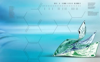
Additive electronics is intrinsically more sustainable than subtractive processes. Yet the current materials are often based on metallic inks and plastic substrates. This is a particular issue in medical wearables with disposable devices. Hence the need to develop sustainable material options
4 minutes read
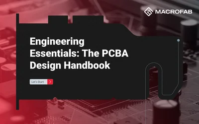
This 75-page e-book will provide you with the design skills to develop exceptional PCBAs that not only meet but surpass their intended objectives.

4 minutes read
An In-depth Analysis of Features, Applications, and Selection Criteria for Embedded Systems Design. Discover the Advantages and Limitations of SPI, I2C, and UART for Efficient Data Exchange in Various Scenarios.
The guide to understanding the state of the art in hardware & software in Edge AI.
Integrated photonics, also known as planar lightwave circuits or integrated optical circuits, revolutionizes optical communication by leveraging the properties of light to process and transmit information. This cutting-edge technology offers superior efficiency and compactness compared to traditional electronic components, paving the way for faster and more energy-efficient communication systems. With its interdisciplinary nature encompassing materials science, quantum physics, and electrical engineering, integrated photonics presents an exciting and promising field of study and research in today's digital era.

Advanced testing methodologies and innovation in semiconductor packaging ensure product reliability in dynamic and harsh operational environments. These strategies are particularly crucial in the rapidly evolving automotive industry.

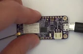
A guide to resources related to the Nordic Semiconductor nRF9160 Development Kit and Soracom connectivity to help you launch your Connect For Good Low Power Wireless Sustainability Challenge submission.
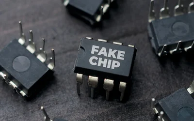
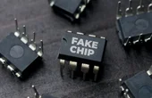
There is a real and growing threat of counterfeit products within the electronics industry. Do you know how to mitigate it?
6 minutes read