
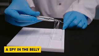
Featuredpodcast
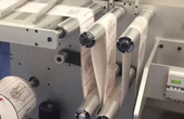
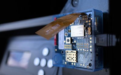
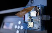
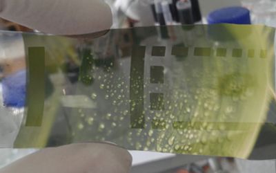
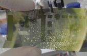
In this episode, we talk about a combined effort between ETH Zurich & the Swiss Federal Lab for Material Science (EMPA) to create “smart” internal bandages for safely patching patients post stomach/intestinal surgery while providing insight to the medical staff about the status of the patch to prevent leakages which can be fatal.