Tented Vias in PCB Design: A Comprehensive Guide to Theory and Best Practices
Discover what tented vias are in PCB design and how to use them effectively – covering their definition, benefits, drawbacks, and best practices from design through manufacturing!

Last updated on 12 Mar, 2025. 25 minutes read
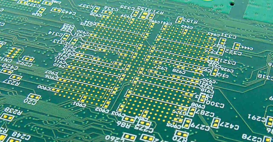
Tented Vias in PCB Design
Introduction
Tented vias are an essential aspect of modern PCB design, offering a reliable solution for enhancing circuit board performance and reliability. These vias are covered with solder mask to prevent contamination, reduce the risk of short circuits, and improve electrical insulation. By eliminating unnecessary exposure to environmental factors, tented vias contribute to enhanced signal integrity and durability, making them a preferred choice in high-density and high-frequency PCB layouts.
Designers implement tented vias to optimize space utilization and protect underlying copper traces, particularly in multilayer PCBs where signal routing is complex. By following industry best practices, engineers can ensure that tented vias contribute to both cost-effective manufacturing and long-term operational stability. This guide explores the theory, applications, and best practices for integrating tented vias into PCB designs effectively.
What Are Tented Vias?
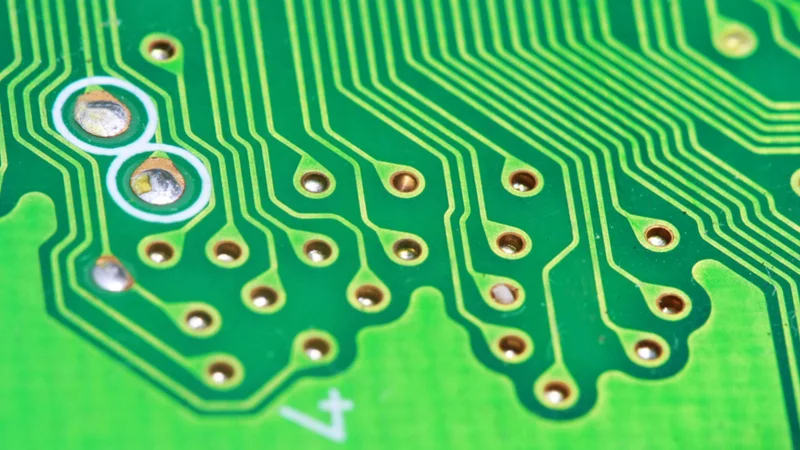
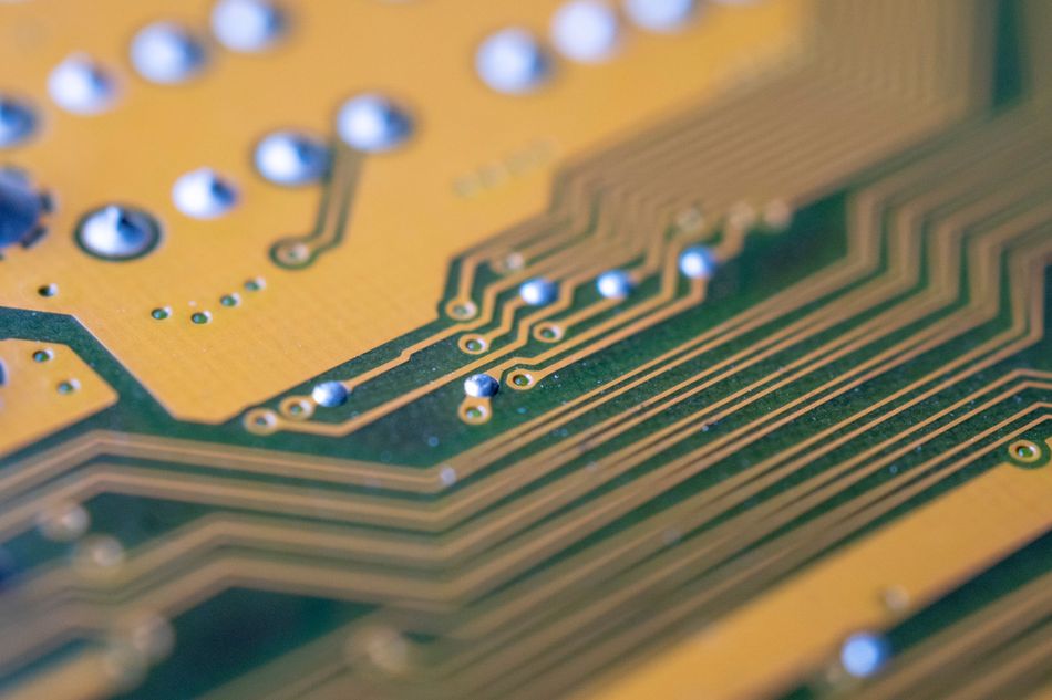
Tented vias are plated through holes in a PCB design that are intentionally covered with a solder mask, either on one or both sides. Unlike standard vias, which have an open clearance in the mask, tented vias are fully or partially enclosed by the solder mask layer, covering the annular ring and, in some cases, sealing the via hole completely. The term “tenting” comes from the solder mask forming a tent-like cover over the via. [1]
The primary purpose of tented vias is to protect the via and surrounding circuitry from contaminants, corrosion, and oxidation, which can lead to short circuits or electrical failures. By enclosing the via under a layer of solder resist, exposure to air, moisture, dust, and flux residues is minimized, increasing the long-term reliability of PCB. If a via remains untented, its exposed copper traces and barrel may be prone to environmental damage, particularly in harsh operating conditions.
Tenting also plays a crucial role in high-density PCB layouts and RF/high-speed circuits. Covering stray copper openings can help reduce electromagnetic coupling, crosstalk, and signal reflections, improving signal integrity in sensitive designs. While the impact of via tenting on electrical performance is typically minor, in high-frequency applications, every measure that enhances isolation contributes to better performance.
Additionally, via tenting is beneficial during PCB assembly, particularly in surface mount designs with fine-pitch components like BGAs and QFNs. An uncovered via near an SMD pad can cause solder wicking, where solder paste is drawn into the hole during reflow, leading to weak solder joints and unreliable connections. By tenting the via, this unwanted solder migration is prevented, ensuring proper adhesion and mechanical strength.
From a PCB manufacturing perspective, tenting is a cost-effective solution that requires no additional fabrication steps beyond standard solder mask application. Tented vias appear as small, masked dots on the board, contributing to a smoother surface finish and improved aesthetics.
Recommended Reading: PCB Via: Essential Guide to Vertical Interconnect Access in Circuit Boards
Types of Vias in PCB Manufacturing
Not all vias are created equal! PCB designers employ different via types depending on board complexity, layer count, and density requirements. Understanding via types helps in deciding which vias might need tenting and how.
Here are the common via types and their roles in PCB manufacturing:
Through-Hole Via (PTH)
A hole drilled all the way through the PCB, plated with copper, connecting the top layer to the bottom layer (and any internal layers in between). This is the most common via type and is integral to the plating process, allowing plating chemicals to circulate during fabrication.
Tenting Considerations: Standard through-hole vias can be tented on one or both sides if needed. They also serve as via for plating process – during fabrication, through-holes allow plating chemicals to circulate. For very large through vias, tenting might be done only after plating is complete, and usually only if the via is small enough for the mask to cover.
Blind Via
A via that connects an outer layer to one or more inner layers but does not go through the entire board (it is “blind” to the other side). Blind vias are used in high-density designs to save space when full-depth drilling isn’t needed.
Tenting Considerations: Blind vias are often tented on the outer surface to prevent solder bridging, oxidation, and solder fill-in during reflow. They start on one of the surfaces and stop at some interior layer. Blind vias often have small diameters (especially in HDI – High Density Interconnect boards) and can be tented on the outer side to, for example, avoid solder fill-in or exposure. Tenting a blind via can protect its opening on the surface without affecting the buried portion.
Buried Via
A via connecting two or more inner layers, completely hidden inside the board (not visible from the outside). Buried vias are manufactured by drilling and plating during sub-lamination steps, and are not visible from the outside.
Tenting Considerations: Since they never open to the PCB surface, the concept of “tenting” doesn’t directly apply – they’re inherently covered by the outer layers. However, their presence can affect how other vias or features are arranged.
Microvia
A very small via (typically laser-drilled and often <=0.15 mm diameter) that usually connects between only adjacent layers (for example, from the top layer to layer 2). Microvias are prevalent in HDI technology and are often placed in component pads (via-in-pad) or in dense BGA breakout areas. [2]
Tenting Considerations: Due to their tiny size, microvias can be completely filled by solder mask in standard processing, effectively self-tenting. Often, microvias in pads are filled with copper or epoxy and plated over (which goes beyond simple tenting). Microvias may also be stacked or staggered in complex boards. Their small size means if you specify no mask opening, they will likely end up covered by default during solder mask application.
Deciding whether to tent, fill, or plug a via depends on its location and function! Through-holes near sensitive components might be candidates for tenting, whereas very large through-holes (like mounting holes or vias used as test points) are usually left open.
Blind and microvias on outer layers can be tented to avoid any openings on the surface, improving board finish and reliability. It’s also worth noting that some PCB design standards (like IPC-2221 and IPC-4761) classify via protection methods for through-holes – including tenting, plugging, and filling – which we will touch on later.
Recommended Reading: Via Types: Essential Guide to Understanding and Utilizing in Electronic Design
Benefits of Tented Vias
Tented vias offer several advantages in PCB design and manufacturing:
Environmental Protection
Covering a via with solder mask shields the annular ring and via barrel from moisture, dust, oxidation, and corrosion. This significantly enhances the long-term durability of a PCB, particularly in harsh environments such as automotive, aerospace, and industrial applications, where exposure to contaminants can degrade copper traces over time. By preventing direct contact with air and chemicals, tented vias help reduce the risk of oxidation and corrosion, extending the lifespan of PCB. For maximum protection, tenting can be combined with conformal coating, providing multiple layers of defense against the environment.
Prevention of Solder Wicking
A critical benefit of tenting vias in PCB assembly is that it prevents solder wicking, where molten solder paste is drawn into an untented via during reflow. This is especially problematic when vias are placed near surface mount pads, such as in BGA or via-in-pad designs.
Without tenting, a via can act like a straw, pulling solder paste away from SMD pads, leading to insufficient solder joints and poor electrical connections. Tenting helps retain solder on the pad, ensuring stronger solder joints and improving assembly yield. In BGA and QFN layouts, designers often tent or plug thermal vias to prevent solder bridging and maintain proper thermal performance.
Reduced Risk of Shorts and Debris Contamination
By covering conductive via areas, tented vias help prevent short circuits caused by stray solder splashes, metal debris, or conductive contaminants. For example, a stray solder splash or a small metal particle on the board can’t enter a tented via or bridge it to nearby copper, because the mask is in the way. The solder mask over the via acts as insulation. This is a reason some high-voltage designs tent vias – to increase insulation distance and prevent any accidental arcing or short via conductive contaminants.
Improved Aesthetics and Cleanliness
Tented vias give the PCB a smoother, cleaner appearance, as you won’t see hundreds of tiny exposed copper rings and holes. The board surface will appear uniformly covered by solder mask except where pads are needed. This is purely a cosmetic/organizational benefit, but in consumer electronics, a uniform look is often preferred. Aesthetic aside, a smooth surface can also aid Automated Optical Inspection (AOI), as there are fewer exposed features to analyze as potential defects. PCB assemblers sometimes appreciate fully masked boards because cleaning under components is easier when vias aren’t trapping residue.
Cost Effectiveness
One of the biggest benefits is that via tenting is essentially free or low-cost to implement. It doesn’t require an extra manufacturing step – it’s accomplished by the normal solder mask application process and by simply having the PCB designer specify no mask opening for those vias. In contrast, other via-sealing methods like plugging or full-filling involve additional materials and process steps.
Tented vias provide a cost-effective and efficient solution for improving PCB durability, soldering reliability, and environmental resistance. By preventing corrosion, solder defects, and electrical shorts, tenting offers valuable protection with minimal impact on manufacturing complexity. However, tenting is not a one-size-fits-all solution! In some cases, other via protection techniques—such as plugging, epoxy filling, or via-in-pad plating—may be required.
Drawbacks of Tented Vias
Despite their advantages, tented vias also come with drawbacks and limitations that designers must consider:
Coverage Limitations and Size Constraints
Tenting works well for small vias, but for larger via diameters, the solder mask may not fully bridge the hole. Typically, vias around 12 mil (0.3 mm) or smaller have the best chance of being completely covered by a standard Liquid Photo Imageable (LPI) solder mask. [3] However, as via diameters increase, the solder mask may partially collapse into the hole or form a weak tent, leading to incomplete protection. In the worst case, mask that flows into a large via could even create a solder void or “solder mask plug” that is not secure and could pop out later.
Best Practice: Tented vias are unreliable for larger holes – beyond a certain diameter, you must assume the hole won’t stay fully covered.
Risk of Trapped Contaminants and Reliability Issues
If a via is tented on one side only, there’s a possibility that flux or cleaning solution from the assembly can get trapped inside the via barrel (since the other end is closed). These trapped residues can be corrosive or conductive over time. Even tenting both sides can trap air or moisture in the via. During soldering or in high-altitude operations, this trapped air may expand (outgas) and potentially cause the solder mask tent to rupture or delaminate. In low-pressure environments (e.g. aerospace applications), outgassing from residues in an unvented via could be problematic.
Best Practice: If a solder mask tent does not adhere well and cracks, any moisture that seeped in can remain inside the via and accelerate corrosion of the copper plating.
Assembly and Testing Constraints
While tenting vias can help with solder assembly in some ways, it can hinder others. Fully tented vias cannot be used as test points on a PCB during In-Circuit Testing (ICT) or probing, since they’re covered by an insulating layer. Test engineers often use exposed via pads for probing, but tenting removes that option unless certain vias are intentionally left untented. In via-in-pad configurations, a tented via under a fine-pitch component pad may create a slight solder mask dome, potentially interfering with flat component seating or proper solder joint formation. If test accessibility is required, leave designated vias untented for probe connections.
Best Practice: For high-density layouts, consider plugging vias rather than tenting them under SMD pads.
Difficulties in Rework or Modifications
If a PCB needs rework or modification, tented vias might complicate the process. For instance, if you needed to solder a wire into a via (as a makeshift repair or bodge), a tented via would first need to be scraped open. Similarly, if you had to drill out a via or measure a signal from it, the mask is an extra hurdle. In contrast, an untented via is readily accessible for rework (you can heat it, add solder, etc.).
Best Practice: Boards that anticipate a lot of manual rework or probing (like in initial prototypes or RF tuning boards) might avoid tenting certain vias.
Potential Solder Mask Issues
Tenting pushes the solder mask application to its limits, which can sometimes result in adhesion failures or manufacturing defects. On dense PCB layouts, narrow solder mask dams between pads and tented vias may break, causing mask slivers to peel off or float around during assembly.
If a tented via is placed too close to an SMD pad, the solder mask might unintentionally bridge the pad, leading to soldering defects. Due to differences in thermal expansion between copper and solder mask, tented vias—especially larger ones—may crack or delaminate after multiple thermal cycles.
Best Practice: Follow PCB fabrication guidelines for minimum solder mask sliver width (typically 4 mil or more) to prevent solder mask failures.
In essence, tented vias are not suitable for every situation! Large vias, vias planned to double as test points, or boards requiring flawless cleaning might not benefit from tenting. The decision to tent should be made case by case, weighing these pros and cons.
Impact on Electrical Performance and PCB Reliability
Tented vias can have subtle effects on the electrical performance of PCB, and some significant effects on its reliability:
Electrical Performance
In most digital and analog circuits, tented vias have little to no impact on signal integrity, as the copper via barrel remains unchanged, and the solder mask layer is merely a thin, non-conductive coating. However, in high-speed digital and RF designs, even small parasitic capacitances or electromagnetic coupling can matter.
By covering the copper of the via, tenting slightly alters the electromagnetic profile: it can reduce electromagnetic radiation or coupling from the via pad – essentially acting like a very thin dielectric cover. While beneficial in reducing unwanted coupling, the mask also slightly increases the capacitance of via to nearby planes, which in high-frequency designs could marginally slow signal edges. In extreme RF applications, designers sometimes simulate the effect of solder mask layers on via performance to ensure minimal disruption to impedance.
Best Practice: While tenting can help reduce crosstalk, it should not be relied upon as the primary method for signal integrity improvements. For critical high-speed designs, via optimization techniques such as backdrilling or via stitching should be considered.
Thermal Performance
Tenting generally does not impact the overall thermal behavior of PCB, but it can restrict heat dissipation in cases where vias are used as thermal paths. If thermal vias (e.g., under a power LED or voltage regulator pad) are fully tented, trapped air prevents solder from filling the via, reducing its ability to transfer heat. Many designers leave one side of thermal vias open so that solder can partially fill the via, improving thermal conductivity while still controlling solder wicking. In high-power applications, vias are often fully filled with conductive epoxy or plated shut (via-in-pad) rather than tented, ensuring efficient thermal transfer.
Best Practice: If vias are part of the thermal dissipation strategy, avoid full tenting and instead opt for selective tenting (one-sided) or filled vias for optimal heat conduction.
Long-Term Reliability
From a reliability standpoint, tenting provides essential corrosion protection but introduces risks if not done properly. Tented vias block exposure to air, moisture, and contaminants, reducing the risk of oxidation inside the via barrel. However, if a tent is weak or cracks, moisture can seep in and accelerate internal corrosion. Poorly applied masks may also trap flux residues, which can be conductive and degrade via reliability over time. In low-pressure environments, air trapped inside tented vias can expand and rupture the mask, causing delamination or contamination issues.
Best Practice: Use high-quality solder masks with strong adhesion to prevent cracking. In harsh environments (marine, aerospace, or industrial settings), consider conformal coating or filled vias instead of simple tenting.
Mechanical Reliability
While tenting does not affect the mechanical strength of the copper plating of via, it does impact solder mask durability under stress. If a via is too large, the solder mask may not form a strong tent, leading to cracks during curing or over time due to thermal expansion cycles. Under extreme temperature variations, the mismatch in expansion rates between copper and solder mask can cause the mask to peel off or form micro-cracks. Pressing on a tented via (e.g., during testing or probing) can dent or tear the mask, exposing the via unintentionally.
Best Practice: For high-reliability applications (military, aerospace, or industrial use), filled and capped vias (per IPC-4761 Type V-VII) are more durable than simple tenting. [4]
Cleaning and Outgassing
One often overlooked aspect is how tented vs. untented vias affect PCB cleaning and post-assembly residue removal. A one-sided tented via may allow flux or cleaning solution to enter but not exit, leading to contamination. Some high-reliability industries (medical, aerospace) require perfectly clean boards. Trapped flux or moisture under a solder mask tent can cause latent failures or short circuits over time. In applications such as space electronics, even microscopic trapped residues inside a tented via can cause serious outgassing problems, leading to device failure.
Best Practice: For vacuum or high-reliability environments, plugged vias or open vias with conformal coating are preferred over basic tenting.
In summary, electrically, tented vias behave almost like normal vias with slight improvements in reducing exposure of copper (which can marginally help signal integrity and EMI). Reliability-wise, tenting is generally a plus as long as it’s within design guidelines (small vias, properly cured mask).
Recommended Reading: Filled Vias: A Comprehensive Guide
Design Considerations and Best Practices for Tented Vias
When deciding to tent vias in your PCB design, keep the following design guidelines and best practices in mind:
Via Size and Tenting Feasibility
Tenting is most effective for small vias, while larger vias are more difficult to fully cover with a solder mask. Vias with a diameter of ≤0.3 mm (12 mil) are generally suitable for full tenting using Liquid Photo Imageable (LPI) solder mask. For such vias, set the solder mask opening (expansion) to 0, or even negative in some CAD tools, so that no clearance is provided and the mask will cover the hole. For larger vias, consider leaving them untented or using alternative methods (like plugging) because the mask likely won’t hold.
If you absolutely must tent a somewhat larger via, consult your fabricator – some can use a dry-film solder mask or special tenting process to cover slightly larger holes, or they might recommend tenting only one side. Finally, the pad size matters: a larger annular ring around a via gives more surface for the mask to adhere, improving the tenting success. Small ring and large hole is the worst-case for tenting, so maintain an adequate annular ring as per design rules.
Best Practice: Limit tenting to small vias and verify the tenting capability of your PCB manufacturer before finalizing the design.
One-Sided vs. Two-Sided Tenting
Decide whether to tent the via on the top side, bottom side, or both. This depends on your goals: If preventing solder wicking from a top-side component pad is the aim, you can tent just the top of the via (solder won’t go down, but the bottom is open for outgassing or test probe if needed). If environmental protection is paramount, tent both sides so the via is fully sealed against moisture and dust. Tenting both sides provides maximum protection, but remember the caution that it also traps anything inside. Many designers tent the top side of all small vias for assembly reasons, and tent the bottom side only for those vias that aren’t needed as test points or connectors.
Best Practice: For assembly-critical vias, tent only the top side to prevent solder wicking while keeping the bottom open for venting or testing.
Placement Near SMT Pads and Components
Proper placement of tented vias near SMT pads and fine-pitch components is crucial for reliable soldering and PCB assembly. If a via is placed too close to an SMD pad, a solder mask dam must be maintained between them. If this mask webbing is too narrow, the openings may merge, exposing unwanted copper and increasing the risk of solder bridging. Microvias in BGA escape routes should be tented or filled to prevent solder wicking. Thermal vias in QFN pads should be tented on the bottom side to keep solder from escaping during reflow soldering. Some designers prefer one-sided tenting to allow top-side solder to flow into the via, forming a solder plug for improved heat dissipation.
Best Practice: Consult with your assembly house on the best via tenting strategy for fine-pitch components. Use assembly notes to specify tenting requirements (e.g., "Tented Vias: all vias ≤12 mil to be tented both sides, except vias in thermal pads where only the bottom is tented.").
Solder Mask Slivers & Minimum Web Distance
Ensure there is sufficient spacing between tented vias and other solder mask openings. Tented vias close to other exposed features can create narrow mask slivers that peel off or flake during manufacturing. The minimum solder mask web distance is typically 4–5 mil. Designers should verify the capability of the PCB fabricator before finalizing via placements. In high-density BGA layouts, vias may need to be tented together, merging solder mask openings into a single continuous mask area for better adhesion. If individual mask dams are too thin, the PCB fabricator may adjust your Gerber files to modify solder mask coverage, so explicitly documenting tenting requirements is recommended.
Best Practice: Use PCB design rules to define solder mask slivers, and include clear fabrication notes to prevent unintended modifications by the manufacturer.
Finally, always review the capabilities and recommendations of the fabricator! Typically, stick to the standard process: tent small vias using the normal solder mask unless a special need arises.
Recommended Reading: Via in Pad PCB Design
Manufacturing Process and Materials for Tented Vias
Tented vias are achieved during the normal PCB fabrication flow, primarily in the solder mask application step. Here’s an overview of how tented vias are implemented in manufacturing and the materials involved:
1. Drilling
First, the PCB is drilled (mechanically or with lasers for microvias) and then through-holes are plated with copper. At this stage, we just have the copper barrels in the board. For tenting, no special action is needed during drilling – except to ensure the via holes meet the size criteria for later tenting.
Fabricators pay attention to hole size and aspect ratio (board thickness to hole diameter) as that can affect plating quality and later how solder mask fills or covers the hole. Clean drilling ensures there are no burs or irregularities that could prevent mask from covering the hole.
2. Copper Plating and Surface Finish
After drilling, vias are copper-plated, and the PCB goes through any surface finish processes (like HASL, ENIG, etc.) before solder mask is applied. It’s worth noting that if a board uses HASL (Hot Air Solder Leveling) as a finish, small untented vias often get filled with solder anyway. But for tented vias, since we’ll be covering them with mask, the finish on the annular ring isn’t critical (it will be covered) – usually, the copper in the via hole will simply be plated and then later covered by mask without additional finish on that portion.
3. Solder Mask Application
This is the critical step for via tenting. There are two main solder mask methods: Liquid Photo Imageable (LPI) Solder Mask and Dry Film Solder Mask.
LPI Solder Mask: In this commonly used method, a liquid polymer solder mask ink is coated over the entire board (by curtain coating, spray, or screen printing). The board is then exposed to UV light with a photolithography process using the solder mask artwork. Wherever the artwork had openings (pads, component lands, etc.), the mask is not cured and will be washed off, exposing copper there. Wherever the artwork was opaque, the mask stays and hardens, covering the copper. To tent a via using LPI, the designer simply does not include a mask opening for that via in the artwork. So the mask remains over the via. The mask may partially enter the via hole due to gravity and viscosity, but typically, for small vias, it just forms a film over the top. After exposure and development, the vias ideally come out fully covered with a solid solder mask. Then the mask is cured (by heat) to fully harden it.
Dry Film Solder Mask: This is a less common approach, but can be used for tenting especially on tiny vias. A dry film mask is a solid sheet that is laminated onto the board. A similar expose-develop process is used: areas to remain masked vs to open are defined. Dry film can sometimes span larger gaps without sagging, so it might achieve tenting on slightly bigger holes more reliably than a liquid mask. Some high-end fabs use a combination: first apply a dry film mask to tent the vias, then apply LPI mask over everything for color and additional coverage (this corresponds to IPC-4761 Type II “tented and covered” vias. The materials here are photopolymer films that adhere during lamination. After curing, the dry film is quite robust!
4. Curing
Once the solder mask (liquid or dry film) is applied and patterned, it is cured—typically by heat (oven bake) or by UV exposure (for certain types). Curing solidifies the mask. For tented vias, an adequate cure is important to ensure the mask adheres around the via and across the hole without lifting later. The curing process is tuned so that even inside the dimples of the via openings the mask is set. Any solvent-based or water-based development process from the previous step is followed by rinsing and drying, so ideally no chemical residues remain in the tented via.
5. Inspection
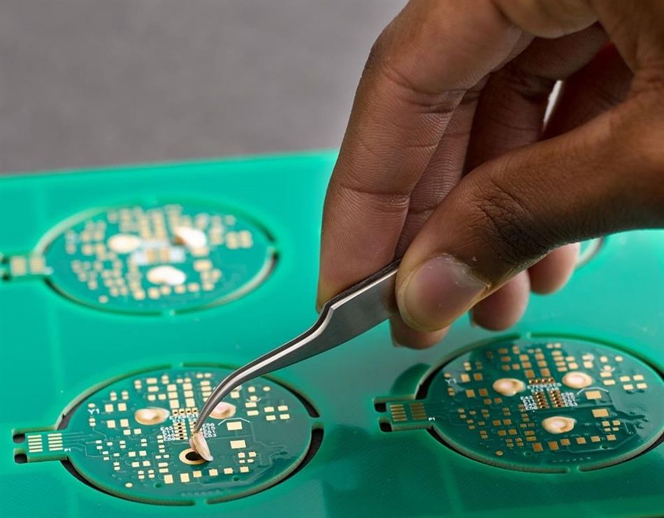
PCB manufacturers will inspect the solder mask layer, often with automated optical inspection (AOI). Tented vias are checked for any openings or voids in the mask. A good fabricator will flag if a via that was supposed to be tented ended up with an opening. They might classify it as an acceptable tiny void or as a defect depending on size. The IPC-A-600 PCB acceptability standard gives guidelines on allowable solder mask coverage and imperfections. [5] In high-rel boards, some customers require no openings in tented vias – hence AOI will catch any pinholes. If issues are found, some fabs might manually touch up mask on a via (though this is rare and usually not done for many vias).
6. Materials
The solder mask itself is the primary material. LPI solder mask inks are typically epoxy-based or polyamide-based polymers with a specific viscosity and resolution. They come in various colors (green is most common due to stability and ease of use). For tenting, mask viscosity, and surface tension are factors – too runny, it falls into holes; too thick, it might leave voids around edges. Fabricators sometimes adjust mask thickness or do double coating for better tenting if needed. Dry film is usually a vacuum-laminated resin film. There is also sometimes the use of non-conductive via fill paste (often an epoxy) if a via is to be filled completely; however, that ventures into via filling/plugging rather than simple tenting. In tenting, we generally don’t introduce any special fill paste – we rely on the mask material itself.
7. Process Variations
If a design specifically requests via plugging or filling, the manufacturer might employ a separate fill step before applying the final solder mask. For example, they may screen-print a thick solder mask or resin into the via holes (this would be via filling), then cure that, and then apply solder mask normally, resulting in what’s effectively filled via with a mask over – which is a different outcome (Type VI filled & covered via) than a simple tent. It’s important to specify correctly: if you say “tented via” the fab will not do an extra fill step; they will just try to cover it with the normal mask. If you require a guaranteed fill, you should specify “filled” or “plugged” vias. We’ll clarify these terms in the comparison section.
Overall, from a manufacturer’s perspective, tented vias are part of the standard workflow and involve no extra fabrication steps, just careful solder mask application. The success of via tenting lies in the quality of the mask process and the design provisions (via size, and spacing) made by the designer. It’s wise to use a fab that has a good track record with fine solder mask features if your design has many tented vias. In the next section, we’ll compare tented vias with others via closure techniques like plugged vias and via-in-pad to highlight when each method is appropriate.
Recommended Reading: PCB Manufacturing Process: A Comprehensive Guide to Understanding and Mastering the Techniques
Tented Vias vs. Plugged Vias vs. Via-in-Pad (Comparison)
Tenting is one approach to covering vias, but there are more robust (albeit costlier) techniques such as via plugging and via-in-pad (filled and capped vias). Here we compare these methods:
Tented Vias
Definition: Via covered by solder mask on one or both sides, without special filling. The via hole may or may not end up completely closed by mask (small vias often do).
Purpose: Primarily to protect and insulate, at low cost.
Pros: Cheapest method (no extra process); provides basic protection against contaminants; prevents solder wicking if tented on the component side; maintains smooth board surface.
Cons: Not guaranteed to seal large holes; mask can crack; not suitable for via in pad on critical components; limited reliability improvement (since hollow inside); not usable as test points once tented.
Typical Use: General PCB designs where via size is small and a little extra protection is desired without added cost – e.g. consumer electronics, moderately dense boards, situations where vias near pads need to be masked off but absolute sealing isn’t required.
Plugged Vias
Definition: Via holes filled with a non-conductive material (such as a specialized solder mask “via fill” paste or resin) and usually capped with solder mask on top.
Purpose: Unlike simple tenting (which might just cover the top), plugging involves actively filling the via barrel, often via a separate screening or vacuum fill process. The fill may not be fully flush; it can leave a slight concave dimple which is then covered by a normal solder mask.
Pros: Ensures the via is completely sealed – no cavity remains, reducing risk of trapped air or contamination. Plugged vias can handle larger diameters than tented because the fill won’t break like a thin mask film would. They also add some structural support inside the via (reducing risk of plating cracks under stress). Assembly-wise, they absolutely stop solder from going through.
Cons: Higher cost – requires extra processing and materials. The filler (often an epoxy) has a different thermal expansion than copper, so reliability is good but extreme thermal cycling can sometimes cause hairline annular cracks (rare with modern materials). If the filler is non-conductive (most are), thermal conductivity through the via is reduced compared to copper – though some fillers have additives to improve this. Plugged vias that aren’t planarized still cannot be used as solderable pads (they’ll have a mask on them), so for via-in-pad usage, you need the next level (capped).
Typical Use: High-density BGA fanouts where vias are very close to pads and tenting might not be reliable, or in boards requiring better reliability than tenting but not necessarily needing to solder on the via. It is also used when a slightly larger vehicle must be closed off – beyond what simple tenting can do. Often specified for via arrays under fine-pitch packages to avoid any solder or flux entrapment (e.g., via fields in RF shields or under modules).
Via-in-Pad (Filled & Capped Vias)
Definition: A via (usually a through via or a micro via) that is drilled in the land/pad of a component, then filled with epoxy or metal and plated over to create a flush, usable pad surface. This is the most advanced via closure – after drilling and plating, the via hole is filled (with either a non-conductive epoxy or a copper fill in some HDI cases), cured, and then a layer of copper plating covers the entire pad, encapsulating the filled via completely. It essentially becomes a solid piece of copper where the via was, allowing the component soldering directly on top.
Pros: Electrically and mechanically optimal – the pad is flat, so solder joints are perfect (no risk of solder going anywhere, as the via is now part of a solid pad). The via is fully sealed and strengthens the pad (as there’s no hollow center under it). This method yields the best results for high-frequency and high reliability because it eliminates via stubs (in high-speed designs, a filled via can be back-drilled or used as a high-speed via without causing reflections as an open stub would). Thermal conduction is also good if a conductive fill or copper plate is used, making it ideal for thermal vias under hotspots.
Cons: Cost is highest – multiple extra steps (fill, cap plating, planarization if needed). Registration and process control need to be precise to ensure the pad remains flat. Sometimes a tiny dimple is visible but within IPC specs for planar height. Also, reworking a board with via-in-pad is hard – you can’t just drill it out easily because it’s solid, but typically you wouldn’t need to unless doing a design change.
Typical Use: Ultra-high density boards (smartphones, CPUs, high-count BGAs) where escape routing forces via-in-pad; RF designs where signal vias need to be as continuous as possible; any design where space is at a premium and the via must share area with a component pad. Also in many mil/aero and HDI applications because of reliability requirements.
Often, a single PCB will employ a mix of these: for example, only the critical BGA via-in-pad are filled and capped, while all other small vias elsewhere are simply tented to save cost.
Cost Implications and Trade-offs
Cost is a deciding factor in choosing via treatment. To recap the cost implications:
Tenting
Virtually, there’s no extra cost! As long as your PCB fabricator doesn’t charge extra for specifying tented vias (most do not, since it’s just part of the mask step), it’s essentially free. You might even save a tiny bit of cost indirectly – a board with many tented vias might use slightly less surface finish material since those via pads aren’t exposed, but that is negligible. The main cost consideration with tenting is yield: if tenting is attempted on too large a via and it fails, you could get defects. But if design rules are followed, tenting is a very economical way to improve a board.
Trade-off: You get cost savings at the expense of not fully guaranteed results for larger holes, and you may accept some reliability risk in extreme conditions. In many cases, this trade-off is acceptable, which is why tented vias are popular in cost-sensitive products.
Plugging
Adds some cost – the PCB manufacturer will perform an extra process (either using a special solder mask via fill in a screening process or vacuum filling with epoxy). This can add to fabrication time and use additional materials. The cost adder can depend on how many vias, their size, and whether one or both sides need plugging. Sometimes, fabs charge by the number of vias to be plugged or a flat surcharge for via plugging service.
Trade-off: Moderate cost increase buys you improved reliability (sealed vias) and possibly the ability to use vias in slightly more demanding situations (like closer to pads or slightly larger holes sealed). If the product demands high reliability and the budget allows, plugging is often worth it. For example, in automotive or industrial equipment, avoiding a field failure may justify the cost. For hobby or low-cost consumer devices, designers often skip plugging unless absolutely needed.
Via-in-Pad (Filled & Capped)
This is typically the most expensive via option! The cost comes not only from filling and plating, but also the required process precision and possible yield loss (if a filled via has voids or the plating isn’t perfect, boards might be scrapped or require rework).
Some fabricators outsource via filling to specialists or use expensive equipment (like planarizing machines or laser drill for filled vias) – all contributing to the cost. However, in high-volume phone or computer production, these costs have been optimized and come down to perhaps a few extra cents per via. In low-volume or prototypes, via-in-pad can sometimes double the PCB fabrication cost because of setup overhead.
Trade-off: You pay a premium to achieve designs that would be impossible otherwise (fine pitch BGAs, etc.) or to ensure maximum reliability. If space and performance demand via-in-pad, the cost is justified because there’s no other choice. But if you can avoid via-in-pad (using dogbone fanout, etc.), you can save a lot. That’s why many designs try tenting or plugging first before resorting to via-in-pad, unless via-in-pad is mandated by component density.
When evaluating these trade-offs, consider the whole product cost and risk. For a mission-critical aerospace board, the cost of via-filling is minimal compared to the cost of potential failure, so tenting might be seen as too risky, and they’ll opt for filled/capped vias per spec. In contrast, for a simple gadget, paying for filled vias would be over-engineering when tenting would do just fine.
Finally, remember that proper design (via sizes, and clearances for mask) will ensure you reap the benefits of tenting without incurring hidden costs like re-spins or board rejections. A little attention during design can save a lot of money and headaches down the line.
Recommended Reading: PCBA Cost and Complexity Design Factors You Should Know
Conclusion
Tented vias play a crucial role in PCB design, offering cost-effective protection against contaminants, corrosion, and solder wicking. By leveraging solder mask application, tenting enhances PCB reliability while maintaining a clean, uniform surface. However, tenting is not always ideal—larger vias, test points, or thermal vias may require plugging or filling instead. Successful implementation depends on proper via sizing, solder mask selection, and fabrication alignment. By following best practices, designers can optimize via protection while ensuring manufacturing consistency. Ultimately, understanding when to tent, plug, or fill vias leads to more reliable and high-performance PCB designs.
Frequently Asked Questions (FAQs)
Q: What does “tenting a via” mean in PCB design?
A: Tenting a via means covering the annular ring and via hole with a solder mask, preventing exposure to air, moisture, and contaminants. The mask forms a tent-like cover, closing the via without using additional materials like epoxy. Tenting can be applied to one or both sides of the PCB to improve reliability, prevent solder wicking, and maintain a clean board surface.
Q: Why should I use tented vias – what are the main benefits?
A: Tented vias improve PCB reliability by protecting vias from corrosion, dust, and oxidation, especially in harsh environments. They also prevent solder wicking, ensuring solder stays on component pads for stronger joints. Additionally, they reduce debris-related shorts and provide a smoother surface, aiding assembly and inspection. Since tenting is done during standard solder mask application, it adds no extra cost.
Q: What are the drawbacks or risks of tenting vias?
A: Tenting has limitations:
1. Large vias may not fully cover, allowing contaminants inside.
2. Solder mask tents can crack or lift, especially under thermal stress.
3. Test points become inaccessible when covered.
4. Trapped flux or moisture in partially tented vias can cause corrosion. Proper via sizing, placement, and solder mask thickness help avoid these issues.
Q: How large can a via be and still be tented successfully?
A: Vias ≤ 12 mil (0.3 mm) are reliably tented with standard solder mask. Larger vias (≥0.5 mm) risk mask sagging or cracking. Some fabricators tent slightly larger vias using dry film solder mask or a dual-layer mask process, but it’s best to confirm manufacturer capabilities. For large vias requiring full closure, plugging or filling is recommended instead of tenting.
References
[1] Cadence. Tented Via: Advantages and Disadvantages [Cited 2025 March 11] Available at: Link
[2] ICAPE. Introduction to HDI PCB Microvias [Cited 2025 March 11] Available at: Link
[3] Sierra Circuits. Solder Mask Layer in PCBs: Top 4 DFM Guidelines [Cited 2025 March 11] Available at: Link
[4] Altium. IPC-4761 Via Types [Cited 2025 March 11] Available at: Link
[5] IPC International. IPC-A-600J - Acceptability of Printed Boards [Cited 2025 March 11] Available at: Link
in this article
1. Introduction2. What Are Tented Vias? 3. Types of Vias in PCB Manufacturing4. Benefits of Tented Vias5. Drawbacks of Tented Vias6. Impact on Electrical Performance and PCB Reliability7. Design Considerations and Best Practices for Tented Vias8. Manufacturing Process and Materials for Tented ViasTented Vias vs. Plugged Vias vs. Via-in-Pad (Comparison)10. Cost Implications and Trade-offs11. Conclusion12. Frequently Asked Questions (FAQs)13. References