ASIC Design: A Step-by-Step Guide from Specification to Silicon
ASIC design is the specialized practice of developing chips tailored to perform specific tasks with maximum efficiency, precision, and reliability—combining architectural insight, hardware expertise, and careful trade-offs to meet exact functional and system-level requirements.

Last updated on 30 May, 2025. 17 minutes read
Introduction
From smartphones and wearables to automotive systems and AI accelerators, custom silicon is the silent workhorse powering today’s most advanced technologies. At the core of many such systems lies the Application-Specific Integrated Circuit (ASIC)—a chip purpose-built to perform a specific function with maximum efficiency.
Recommended reading: What is an ASIC: A Comprehensive Guide to Understanding Application-Specific Integrated Circuits
Unlike general-purpose processors or reconfigurable, programmable platforms like Field-Programmable Gate Arrays (FPGAs), custom ASICs are fixed in functionality once fabricated. While FPGAs are well-suited for prototyping and mixed-signal validation, ASICs offer a cost-effective, high-efficiency solution for dedicated applications. This fixed nature enables superior performance and energy efficiency but also makes the design process more complex, time-intensive, and costly. Successful ASIC development demands precise planning, a solid understanding of logic design and circuit design, and a well-structured flow that spans specification, coding, verification, and physical implementation.
Recommended reading: ASIC vs FPGA: A Comprehensive Comparison
This article provides a structured walkthrough of the ASIC design journey. We’ll explore each major stage, define key technical concepts, and highlight the decisions and trade-offs that shape the final silicon. Whether you're stepping into chip design or revisiting foundational principles, this guide aims to be both accessible and technically rigorous.
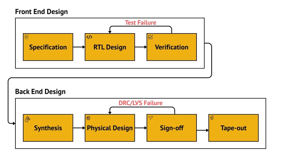
Overview of the ASIC Design Process
Designing an ASIC is not a linear activity—it’s a sequence of highly interdependent phases that involve specification, coding, simulation, optimization, physical layout, and finally, manufacturing handoff. Each stage feeds into the next, with feedback loops that allow designers to catch and fix issues early before they become costly.
At a high level, the ASIC design flow includes:
Capturing the design intent through detailed specifications
Describing the functionality in hardware description languages like Verilog or Very High-Speed Integrated Circuit Hardware Definition Language (VHDL)
Verifying that the logic behaves correctly
Converting the Register Transfer Level (RTL) code into logic gates using synthesis tools
Physically laying out the gates, interconnects, power, and clock networks
Validating the final layout for timing, manufacturability, and power
Sending the final layout to the foundry for fabrication
Below is a flowchart that outlines this full process from concept to silicon:
Defining Design Goals
Every ASIC design begins with a clear understanding of what the chip must accomplish and under what constraints. These early decisions shape the architecture, tools, and trade-offs that follow throughout the design process.
At the heart of this stage is a triad known as PPA—Performance, Power, and Area. These three parameters are tightly linked and must be balanced based on the target application.
Performance: How fast the chip operates. Typically measured in clock frequency (MHz/GHz) or throughput (e.g., data processed per second).
Power: How much energy the chip consumes, including:
Dynamic power, from transistor switching activity during operation
Static power, from leakage currents even when idle
Area: The physical silicon space the design occupies, which impacts cost and yield during manufacturing.
Improving one usually affects the others. For instance, increasing clock speed may require more logic gates, raising both area and power consumption. The designer’s job is to find the right balance, depending on whether speed, energy efficiency, or size is the top priority.
Another early decision is selecting the technology node, which refers to the scale of transistors used in fabrication. Nodes are named by feature size—such as 90 nm, 28 nm, or 5 nm.
Recommended reading: Understanding Transistors: What They Are and How They Work
At smaller nodes (7 nm and below), chips are typically built using Fin Field-Effect Transistor (FinFET) structures instead of traditional planar Complementary Metal-Oxide-Semiconductor (CMOS) transistors. These advanced nodes require tighter design rules, specialized standard cell libraries, and more advanced Electronic Design Automation (EDA) tool support—increasing both design complexity and tool dependency.
Smaller nodes provide:
Higher transistor density
Better power efficiency
Faster switching speeds
But they also bring:
Greater design complexity
Higher fabrication cost
Stricter timing and layout rules
Choosing a node depends on factors like performance needs, product lifespan, cost targets, and tool availability.
Alongside technical goals, the team defines what the chip must functionally do. This includes specific features—like image encoding, signal filtering, or secure data processing—and how those features must behave.
Also important are non-functional constraints, such as:
Latency requirements (e.g., must respond within 10 ms)
Operating voltage and temperature range
On-chip memory requirements (e.g., 512 KB SRAM)
Interface and communication standards (e.g., PCIe, I2C, SPI)
In most cases, designers don’t build everything from scratch. They rely on IP blocks—pre-designed modules like memory controllers, I/O interfaces, or processor cores—to reduce time and complexity. IP reuse offers benefits such as:
Shorter design cycles
Lower verification effort
Reduced risk of functional bugs
Many ASICs follow a semi-custom design style, using standard building blocks to balance time and cost while achieving high-performance outcomes. However, integrating third-party IP also introduces potential compatibility and licensing concerns.
Finally, there’s the business-side constraint: time-to-market. Releasing a chip too late can mean missing a product cycle or losing competitive advantage. This pressure affects decisions on IP reuse, design scope, and resource allocation.
With all these goals and constraints clarified, the next step is to formalize them into a specification—a document that guides the team from concept to implementation.
Specification and Planning
Once the design goals are defined, the next step is to convert them into a detailed specification—a structured document that captures both what the chip must do and how it should be built. This is not just a checklist of features; it’s the foundation upon which the entire project is constructed.
At the highest level, the specification identifies the chip’s functionality, interfaces, and performance targets. It also outlines architectural expectations, integration plans, and assumptions about the system the ASIC will live in. A well-written specification saves time and reduces miscommunication between teams working on different parts of the project.
A typical specification includes:
Functional description: What the chip should do, including input-output behavior, supported operations, and data formats.
Non-functional requirements: Power budget, timing constraints, area limits, and environmental tolerances.
Interfaces: Communication protocols and pin-level descriptions (e.g., UART, I2C, PCIe).
Memory map: Address layout for internal registers or embedded memory blocks.
Clock and reset strategy: Number of clock domains, reset behavior, and startup sequencing.
These details are written at a system level, meaning they describe what the chip should do—not how it’s implemented. This allows architects and designers to independently explore different microarchitectural approaches.
This is also the phase where engineers begin partitioning the design. Large systems are broken into smaller, manageable blocks or subsystems. Each block will later become its own RTL module, tested independently before integration.
Design partitioning considers:
Logical boundaries (e.g., control path vs data path)
Interface clarity between blocks
Reusability of certain modules
Timing and physical proximity in the final layout
The distinction between architecture and microarchitecture becomes critical at this stage. Architecture refers to the high-level behavior of the system—what blocks exist and how they interact. Microarchitecture focuses on how each block works internally—its pipelines, state machines, and data paths.
Another important planning consideration is tool compatibility and EDA flow. Teams often lock in a toolchain—like Synopsys, Cadence, or Siemens EDA—based on team familiarity, licensing, and support for the chosen technology node. Tool flow consistency is essential, as mismatched tools can create translation issues or affect simulation accuracy.
By the end of this stage, the team has a design specification, a block diagram, an architectural strategy, and an early verification plan. With these in place, the actual design work can begin—starting with the creation of the Register Transfer Level description.
RTL Design and Coding Practices
Once the system architecture and block-level planning are complete, designers begin implementing the chip’s functionality in a hardware description language (HDL). The most common choices are Verilog and VHDL, and the description is written at the RTL—an abstraction that models how data flows between storage elements (registers) under the control of a clock.
Recommended reading: Verilog vs VHDL: A Comprehensive Comparison
RTL design is the digital equivalent of writing the source code of a chip. It doesn’t describe physical layout or silicon geometry—instead, it defines how the system behaves in each clock cycle. RTL describes how data moves between registers and how logic design captures control and data flow, often driven by the system’s underlying algorithm.
Most modern ASICs use synchronous design, meaning that all operations are coordinated using a clock signal. Data moves between registers only on specific edges (rising or falling) of the clock, ensuring predictable and analyzable behavior.
Here’s a simple example in Verilog showing a register that stores a value:
always @(posedge clk) begin
  out <= in;
end
This describes a basic D flip-flop—a one-bit memory element that captures the input in on each rising edge of the clock and stores it in out.
When describing such logic in Verilog, designers follow certain conventions:
Use non-blocking assignments (<=) for sequential logic (like registers)
Use blocking assignments (=) for combinational logic (like simple if-else decisions)
For example, here’s a basic combinational block:
always @(*) begin
  if (sel)
    out = a;
  else
    out = b;
end
This is a 2-to-1 multiplexer—it chooses between inputs a and b based on the value of sel. The @(*) sensitivity list tells the simulator to evaluate the block whenever any input changes.
Another common structure is the Finite State Machine (FSM), used for control flow. Here’s a simplified example:
always @(posedge clk) begin
  if (reset)
    state <= 0;
  else if (start)
    state <= 1;
end
This represents a basic state transition between an idle and active state based on control signals reset and start.
As designs grow in complexity, they are divided into smaller, reusable modules. Each module performs a specific function and communicates with others through clearly defined inputs and outputs. Writing clean, modular RTL code helps not just with readability, but also with debugging, testing, and eventual synthesis.
At this stage, the focus is on ensuring the RTL code reflects the design intent. But before translating it into logic gates, engineers need to verify that it works under all conditions. That’s where the next phase—functional verification—comes in.
Functional Verification
Once the RTL code is written, the next step is to check whether it behaves as expected. This is called functional verification, and it’s one of the most critical (and time-consuming) stages in ASIC design. A single missed bug at this stage can lead to a non-working chip after fabrication—something that’s not only expensive to fix but often impossible.
Functional verification is usually done through simulation, which mimics how the design will behave in hardware. Instead of building the chip physically, simulation tools execute the RTL code and show how signals change over time in response to inputs.
To test a design, engineers write a testbench—a separate piece of code that provides inputs to the design and checks the outputs. Think of it as a virtual lab setup that stimulates the circuit and watches how it reacts.
Here’s a very simple example. Suppose we have a 2-input AND gate module:
module and_gate(input a, input b, output y);
  assign y = a & b;
endmodule
A minimal testbench for this module might look like:
module tb;
  reg a, b;
  wire y;
  and_gate uut (.a(a), .b(b), .y(y));
  initial begin
    a = 0; b = 0;
    #10 a = 1;
    #10 b = 1;
    #10 a = 0;
  end
endmodule
This testbench applies different combinations of inputs to the AND gate and lets the simulation run, showing how the output responds.
To improve test coverage, engineers use:
Waveform viewers to observe signal changes over time
Assertions, which check that certain conditions are always true (e.g., “output must be high when both inputs are high”)
Code coverage tools, which report how much of the RTL code was exercised during simulation
In large projects, functional verification often involves test scenarios that are:
Directed: Manually written for known edge cases or corner conditions
Constrained-random: Inputs are generated randomly within defined bounds to explore unexpected behaviors
For more advanced verification, teams may use structured environments like SystemVerilog with Universal Verification Methodology (UVM). These frameworks support reusable test components, scoreboards, and automated checking—but they’re generally introduced at the industry level or in advanced coursework.
Recommended reading: Guide to Mastering SystemVerilog: Elevate Your Hardware Design and Verification Skills
The goal at this stage is to catch functional issues early—before the design is converted to gates or passed on to layout. Once the design behaves correctly in simulation across all expected conditions, it’s ready for the next major phase: synthesis.
Synthesis and Timing Analysis
With a functionally correct RTL design in place, the next step is to convert it into a form that can be physically implemented on silicon. This process is known as logic synthesis.
In synthesis, the hardware description written in Verilog or VHDL is translated into a gate-level netlist—a detailed map of logic gates (like AND, OR, NOT, flip-flops) that can be physically laid out on the chip. The synthesis tool works with a library of available gates provided by the semiconductor foundry, each with known properties like speed, power, and area.
This transformation is handled by synthesis tools such as Synopsys Design Compiler or Cadence Genus. These tools don’t just convert RTL to gates—they also try to optimize the design based on constraints set by the engineer.
Typical constraints include:
Clock frequency (e.g., the design must operate at 200 MHz)
Maximum area the logic can occupy
Power limits for dynamic and static consumption
Input-output delays to account for signals entering and exiting the chip
The result of synthesis is a netlist—a file that lists every gate and how it's connected. But having a gate-level design isn't enough. Engineers must now verify that signals will arrive at their destinations on time. That’s where static timing analysis (STA) comes in.
STA checks the timing paths in the design and ensures that signals have enough time to propagate between registers within a single clock cycle. It calculates the delays through logic gates and wires and compares them with the available time dictated by the clock frequency.
The key timing checks include:
Setup time: The minimum time before the clock edge that data must be stable
Hold time: The minimum time after the clock edge that data must remain stable
Slack: The difference between the required time and the actual time a signal takes. Positive slack means the path meets timing; negative slack means it’s too slow.
For example, if your design must run at 200 MHz (5 ns clock period), and a signal takes 4.3 ns to travel from one flip-flop to the next, the slack is +0.7 ns—safe. But if it takes 5.6 ns, the slack is -0.6 ns—timing violation.
Fixing timing violations may involve:
Reorganizing logic to reduce levels of gates in critical paths
Register balancing or pipelining
Using faster gates from the library
Rewriting inefficient RTL segments
This process of tuning the design to meet timing is called timing closure, and it’s one of the most important goals before handing off the netlist to physical design.
Synthesis and STA act as a bridge between functional correctness and physical feasibility. Once timing is met and the design is stable, the focus shifts to building the actual layout on silicon.
Power and Clock Management
Modern ASICs are expected to do more while consuming less. Whether it’s a smartphone SoC or a wearable sensor controller, power consumption is often as critical as performance. Left unmanaged, excessive power leads to overheating, shorter battery life, and reduced reliability. That’s why power optimization is built into the design flow from an early stage.
Types of Power Consumption
There are two main types of power in digital circuits:
Dynamic power: Caused by switching activity—when transistors turn on and off as signals change. It increases with frequency and the amount of logic toggling on each clock cycle.
Static power: Caused by leakage currents, which flow through transistors even when they’re not switching. This becomes more prominent at smaller technology nodes.
Low-Power Design Techniques
To manage both dynamic and static power, designers use a variety of techniques. Here are a few commonly used ones:
Clock gating: The clock is one of the most power-hungry signals in a chip. Clock gating temporarily disables the clock to parts of the circuit that aren’t needed, reducing unnecessary switching.
Recommended reading: Clock Gating: Powering Down Idle Circuits
Example:
if (enable)
  clk_out = clk;
else
  clk_out = 0;
Power gating: Involves completely shutting off power to blocks when not in use. This requires isolation cells and special control logic, but significantly reduces leakage power.
Multi-voltage domains: Different parts of the chip run at different voltages depending on performance needs. For example, a fast core may run at 1.0V while a low-power sensor block operates at 0.8V.
Operand isolation: Prevents unnecessary logic evaluation by freezing signal paths unless required.
To manage these techniques, engineers may define power intent separately using formats like Unified Power Format (UPF) or Common Power Format (CPF). These tell tools how power domains, switches, and isolation logic should be implemented.
Clock Domain Crossing (CDC)
Large ASICs often use multiple clock domains—meaning different parts of the chip operate at different frequencies or phases. While this helps optimize performance and power, it introduces new challenges.
Signals moving between clock domains can cause metastability—a condition where a flip-flop output becomes unpredictable due to insufficient setup or hold time.
To prevent this, designers use synchronizers, such as:
Two-stage flip-flop synchronizers: Used for single-bit signals
Asynchronous FIFOs: Used for multi-bit data transfers across domains
Here’s a simple two-flip-flop synchronizer for a signal crossing into a faster clock domain:
always @(posedge clk_fast) begin
  sync_1 <= async_in;
  sync_2 <= sync_1;
end
This reduces the chance of metastability by allowing the signal to settle before being used.
In large or safety-critical designs, formal verification tools like Questa CDC or SpyGlass CDC are often used to detect asynchronous crossings, missing synchronizers, or handshake mismatches early in the flow.
Managing power and clock domains adds complexity, but it’s necessary for building scalable and energy-efficient chips. These techniques are especially relevant when targeting mobile, edge, or battery-powered applications.
Once power and timing domains are planned and verified, the design is ready to move into physical realization—floorplanning, placement, and routing on the silicon itself.
Physical Design and Layout
After the design is synthesized and meets timing and power requirements, it’s time to build its physical form—the actual layout that will be printed onto the silicon wafer. This stage is known as physical design, and it turns the abstract netlist of gates and flip-flops into a concrete arrangement of shapes, wires, and layers that a fabrication facility can manufacture.
Recommended reading: Silicon Wafers: Production, Properties and Application
Think of it like going from a circuit diagram to a floor plan for construction—except instead of bricks and walls, you’re placing transistors, routing metal layers, and designing power grids.
Key Stages in Physical Design
The physical design flow includes several key steps:
Floorplanning: Defines the top-level layout of the chip. Designers decide where large functional blocks (like memory, ALUs, or I/O controllers) will be placed. It also allocates space for clock and power routing, buffers, and I/O pads.
Placement: Positions all the standard cells—these are the basic logic gates like AND, OR, flip-flops—within each block. The goal is to optimize for signal timing, area, and minimal wire congestion.
Clock Tree Synthesis (CTS): Distributes the clock signal evenly to all flip-flops. Since the clock needs to arrive at different parts of the chip at nearly the same time, CTS inserts buffers and routing to balance delays and minimize clock skew (timing differences between clock arrival at different points).
Recommended reading: PCB Via: Essential Guide to Vertical Interconnect Access in Circuit Boards
Routing: Connects all placed cells using metal wires across multiple layers. Modern chips may use 6–15 metal layers for routing, depending on complexity. Routing also includes via placement—tiny vertical connections between metal layers. The place and route phase ensures gates are efficiently organized and routed—especially in dense system-on-chip or single-chip implementations.
Power planning: Involves designing power grids and adding decoupling capacitors to stabilize voltage during switching. Proper power distribution is crucial to avoid IR drops or electromigration (gradual wire damage from current).
Physical Verification: Once the layout is complete, tools check the design for fabrication readiness using two key checks:
Design Rule Check (DRC): Verifies that the layout follows all manufacturing rules (like minimum spacing between wires).
Layout vs Schematic (LVS): Ensures the layout matches the logical circuit. It confirms that no connections were missed or misrouted.
Parasitics and Extraction
When wires are added, they introduce parasitic effects—like resistance and capacitance—which impact signal delay and power. Tools perform RC extraction to model these effects accurately. Timing is then re-analyzed using post-layout timing analysis, which is more accurate than pre-layout estimates.
Final Output: GDSII
After layout and verification, the design is exported as a Graphic Data System II (GDSII) file—an industry standard format used by semiconductor foundries to fabricate the chip. It contains all geometric data: transistors, routing, metal layers, and masks needed to print the design onto wafers.
At this point, the physical implementation of the ASIC is complete. But before the design is sent for fabrication, it must also be made testable—so that any manufacturing defects can be detected after production.
Sign-off
Before an ASIC design is sent for fabrication, it must pass a series of critical checks to ensure it is both functionally correct and manufacturable. This stage—called sign-off—includes a variety of analyses that verify timing, power, layout integrity, and testability.
One essential component is Design for Testability (DFT). Because chips can develop microscopic defects during manufacturing, designers include test logic to make faults easier to detect and isolate.
Scan chains are widely used for this purpose. They link flip-flops into shift-register paths, allowing external tools to scan in test values and scan out results—giving visibility into the chip’s internal logic without needing physical probes. This enables detection of common manufacturing faults like stuck-at-0 or stuck-at-1 conditions.
In addition to scan chains, many designs include Built-In Self-Test (BIST) logic:
Memory BIST (MBIST) tests embedded memory blocks for stuck bits or address decoder errors.
Logic BIST (LBIST) checks digital logic using internal pattern generators and comparators.
To support board-level diagnostics, chips may also implement boundary scan using the Joint Test Action Group (JTAG) standard. This enables testing of chip-to-chip interconnects and access to internal test logic without relying on physical pin-level debugging.
Final sign-off also involves:
Test coverage analysis to ensure internal logic can be adequately observed and controlled
Yield estimation to predict the percentage of defect-free chips
Redundancy insertion (e.g., spare memory rows or columns) to improve yield recoverability
IR drop analysis, electromigration checks, and crosstalk noise estimation to ensure long-term signal integrity and physical reliability
Once the design has cleared all functional, timing, DRC, LVS, and test-related checks, it is considered ready for tape-out.
Tape-out
Tape-out is the final step in the ASIC design process—the point where design data is frozen and sent to the fabrication facility. The term originates from the era when design files were literally stored on magnetic tape, though today it's a digital handoff.
The design is exported in a standardized format, typically GDSII or Open Artwork System Interchange Standard (OASIS), which contains all physical layout information: transistors, routing, metal layers, and mask data.
Along with the layout file, teams also deliver:
Test patterns for production-line validation
Documentation for packaging and bring-up
Manufacturing-specific metadata (e.g., corner cases, lot definitions)
After tape-out, silicon wafers are fabricated, packaged, and returned to the engineering team for bring-up—the process of validating functionality on real hardware. If the chip performs as expected under operating conditions, it moves into volume production.
Case Snapshot: An ASIC in Practice
To bring all these concepts together, let’s walk through a simplified example of how a real-world ASIC might be designed. Suppose a company wants to create a low-power image processing chip for a compact drone camera. The chip must take raw pixel data from a sensor, apply basic filters, compress the image, and send the output over a wireless interface.
The design team begins by defining clear goals:
Performance: Process 30 frames per second at VGA resolution (640x480 pixels)
Power: Stay under 150 mW for longer flight time
Area: Small enough to fit inside a lightweight module
Interfaces: Connect to camera sensor and transmit over Serial Peripheral Interface (SPI) or Universal Asynchronous Receiver/Transmitter (UART)
Based on these, the architecture is planned with blocks for:
Sensor input buffering
A simple edge-detection filter
A lightweight compression engine
SPI controller for output
Power management and clock gating logic
Each block is described in Verilog at the RTL level, using clean modular code. The filter, for instance, might be pipelined to process a pixel every clock cycle, and the compression block reuses IP from a previous project.
Once RTL coding is complete, the team writes testbenches to simulate typical image streams and validate output correctness. Bugs are fixed during simulation before synthesis begins.
During synthesis, some timing violations are detected in the compression block. The team adds pipeline stages to balance logic depth and improve timing. After timing closure, physical design is performed. The floorplan places the high-activity blocks close together to minimize routing delay, and clock tree synthesis ensures synchronized operation across the chip.
Power-aware design is emphasized throughout. The SPI output block is gated when idle, and unused logic during sensor blanking intervals is shut off via power gating. Static timing analysis and parasitic extraction confirm that all paths meet timing after layout.
Before tape-out, scan chains and BIST are added to test logic and embedded memory. The final chip layout is packaged into a GDSII file and sent for fabrication.

Weeks later, the team receives silicon samples and runs lab tests. The chip meets its performance and power goals, and after minor firmware adjustments, it enters volume production—ready to fly in thousands of compact drone cameras.
Conclusion
Designing an ASIC is a journey that begins with an idea and ends with silicon—passing through layers of abstraction, optimization, and precision engineering. Each stage in the process, from specification and RTL development to verification, synthesis, layout, and test preparation, demands careful planning and collaboration. It's a process that leaves little room for error, but when done right, the result is a chip that delivers unmatched efficiency, performance, and specialization.
Understanding the ASIC flow helps engineers appreciate how every decision—technical or architectural—has ripple effects on power, timing, area, and manufacturability. Even at the undergraduate level, developing a strong grasp of these fundamentals builds the foundation for deeper work in digital design, VLSI, or semiconductor product development.
As technology continues to push boundaries in AI, communications, and edge computing, ASIC chips will remain central to innovation. For those who master this process, the ability to shape custom hardware from logic to layout is both a technical skill and an engineering craft.
Frequently Asked Questions
What is the difference between an ASIC and an FPGA?
ASICs and FPGAs serve different purposes in electronic design. ASICs are custom-designed for a specific application, offering optimized performance and power efficiency, but they are fixed once fabricated. FPGAs, on the other hand, are reprogrammable and suitable for prototyping or applications requiring flexibility.
Feature | ASIC | FPGA |
Flexibility | Fixed functionality | Reconfigurable after fabrication |
Cost | High upfront cost, lower per-unit for high volume | Lower upfront cost, higher per-unit |
Performance | Optimized for speed and efficiency | Generally slower, consumes more power |
Use Case | High-volume production, power-sensitive applications | Prototyping, low-volume applications, flexible designs |
How long does it take to design and produce an ASIC?
The ASIC development process typically takes 12 to 24 months, depending on complexity and team size. Several factors can extend or shorten this timeline:
Complexity: High-performance chips with advanced features require longer development.
Verification Time: Extensive testing and validation ensure correctness, which can take months.
Fabrication & Packaging: Manufacturing, wafer production, and packaging add additional lead time.
Potential Respins: Errors discovered late in the process can cause costly and time-consuming design revisions.
What tools and languages are commonly used?
ASIC design relies on specialized HDLs and Electronic Design Automation (EDA) tools for various stages:
HDLs:
Verilog, VHDL, SystemVerilog (used for RTL design and verification)
EDA Tools:
Simulation & Verification: ModelSim, Questa, VCS
Synthesis: Synopsys Design Compiler, Cadence Genus
Place & Route: Cadence Innovus, Synopsys ICC2
Timing Analysis: PrimeTime, Tempus
Physical Verification: Calibre, PVS
Why are ASICs expensive, and when are they worth it?
ASICs require significant upfront investment due to:
Mask Costs: Custom photolithography masks for fabrication are expensive.
EDA Tool Licenses: High costs associated with design and verification tools.
Engineering Effort: Complex designs require experienced engineers over long development cycles.
However, ASICs are cost-effective for high-volume production, where the per-unit cost becomes significantly lower compared to alternatives like FPGAs. They also provide unmatched performance, power efficiency, and integration for applications such as smartphones, data centers, and automotive systems.
What are the key factors to consider when selecting a semiconductor foundry for ASIC manufacturing?
Important factors to consider when choosing a foundry include their experience, technical capabilities, capacity, and track record in the industry. Additionally, designers should evaluate the foundry's support for the chosen fabrication technology and their ability to meet the performance, power, and cost targets for the ASIC.
References
[1] Taraate V. ASIC Design and Synthesis: RTL Design Using Verilog. Singapore: Springer; 2021.
[2] Smith MJ. Application-Specific Integrated Circuits. Boston: Addison-Wesley; 1997.
[3] Rabaey JM, Chandrakasan A, Nikolić B. Digital Integrated Circuits: A Design Perspective. 2nd ed. Upper Saddle River (NJ): Prentice Hall; 2003.
[4] Weste NEH, Harris D. CMOS VLSI Design: A Circuits and Systems Perspective. 4th ed. Boston: Addison-Wesley; 2010.
[5] Palnitkar S. Verilog HDL: A Guide to Digital Design and Synthesis. 2nd ed. Upper Saddle River (NJ): Prentice Hall; 2003.
[6] Vahid F. Digital Design with RTL Design, VHDL, and Verilog. 2nd ed. Hoboken (NJ): Wiley; 2010.
in this article
1. Introduction2. Overview of the ASIC Design Process3. Defining Design Goals4. Specification and Planning5. RTL Design and Coding Practices6. Functional Verification7. Synthesis and Timing Analysis8. Power and Clock Management9. Physical Design and Layout10. Sign-off11. Tape-out12. Case Snapshot: An ASIC in Practice13. Conclusion14. Frequently Asked Questions15. References