What Is an FPGA? Complete Guide to Field Programmable Gate Arrays for Engineers
Discover what is an FPGA and how field-programmable gate arrays empower engineers to create custom digital hardware. This guide combines a beginner-friendly definition with architectural insights, process technology, and design methodologies.

Last updated on 01 Jun, 2026. 17 minutes read
ASIC, FPGA
Key Takeaways
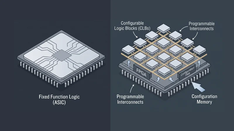
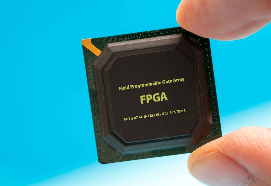
What Is an FPGA? A field‑programmable gate array (FPGA) is an integrated circuit that can be configured by the user after manufacturing. Programming an FPGA loads a bitstream that defines hardware functions, rather than instructions, to implement digital circuits.
Granular Hardware Building Blocks: Modern FPGAs consist of configurable logic blocks (CLBs) made from look‑up tables (LUTs), flip‑flops and multiplexers, block RAM, DSP slices, high‑speed transceivers and configurable I/O. These resources support both general‑purpose logic and specialized functions such as high‑speed signal processing.
Parallel, Low‑Latency Processing: Unlike CPUs or GPUs, FPGAs execute operations in deeply pipelined hardware. Thousands of small processing units (adaptive logic modules, memory blocks and DSP blocks) can operate simultaneously, enabling microsecond‑scale latency for signal processing, AI inference and communications.
Design Flow Mirrors ASIC Design but with Lower Risk: FPGA projects still follow a rigorous design flow of HDL coding, simulation, synthesis, implementation, and debugging, but they avoid the high non‑recurring engineering (NRE) costs of ASICs. FPGAs can be reprogrammed throughout development and deployment, allowing field upgrades and feature additions.
Choose the Right Technology: FPGAs offer flexibility and parallelism, ASICs deliver maximum efficiency, CPUs and GPUs suit software‑centric tasks, and microcontrollers provide simple, low‑power control. Understanding these trade‑offs helps engineers select the best platform for a given application.
Introduction
FPGAs bridge the gap between fixed‑function integrated circuits and general‑purpose processors. The Field-Programmable Gate Array (FPGA) is an integrated circuit that designers or end users configure after fabrication. Instead of executing instructions sequentially like a CPU, an FPGA implements digital logic directly in hardware. What is an FPGA? In practical terms, it is a flexible hardware platform built from configurable logic blocks, programmable interconnects, input/output blocks, memory resources, DSP slices, and high-speed interfaces.
Engineers define FPGA behavior using hardware description languages such as Verilog or VHDL, then generate a bitstream to program the device. What is an FPGA? It is a bridge between fixed-function ASICs and general-purpose processors, offering both performance and adaptability. Still curious about, what is an FPGA? It is a critical technology for telecommunications, aerospace, automotive systems, industrial automation, AI acceleration, and rapid hardware prototyping.
Understanding FPGA Basics
What Is an FPGA?
The field‑programmable gate array (FPGA) is an integrated circuit designed to be configured by the user after manufacturing [1]. FPGAs originated in the 1980s as programmable logic arrays and evolved into today’s high‑density devices containing millions of logic elements and specialized hard IP blocks. The name reflects both their programmable nature - field‑programmable - and their structure - a gate array of configurable logic.
The same device can implement a digital filter one day and an AI accelerator the next. This flexibility has made FPGAs a key component in prototyping, low‑ and medium‑volume production, and systems that require frequent updates. Market analysts estimate that the global FPGA market is projected to reach US$ 27.51 billion by 2032, driven by demand from AI/ML, 5G, and IoT applications [2].
Components of an FPGA
FPGAs derive their versatility from a rich set of configurable and fixed hardware resources. The main components of an FPGA are:
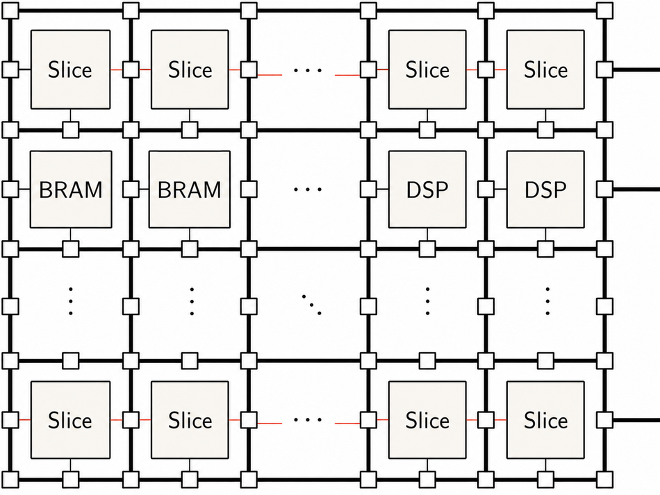
Configurable Logic Blocks (CLBs) and Slices
CLBs are the fundamental computational units of the FPGA. Each CLB comprises multiple slices containing LUTs, flip‑flops, multiplexers and dedicated carry logic.
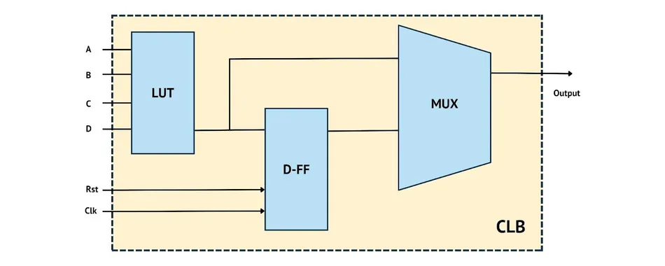
In Xilinx 7‑series devices, a CLB contains two slices (SLICEL and SLICEM); each slice hosts four 6‑input LUTs and eight flip‑flops [3]. CLB thus consists of eight LUTs and sixteen flip‑flops. SLICEM slices allow LUTs to be configured as distributed RAM or shift registers, providing small amounts of on‑chip memory.
Look‑Up Tables (LUTs)
LUTs implement combinational logic by storing output values for every possible input combination. In typical FPGAs, each LUT has six inputs and two outputs, allowing it to implement one six‑input function or two five‑input functions with shared inputs. Designers combine LUTs through the interconnect network to build larger logic functions, including multiplexers and arithmetic units.
Flip‑Flops and Latches
Flip‑flops (FFs) provide one‑bit storage for sequential logic. Each slice contains eight flip‑flops, four of which are dedicated synchronous storage elements; the other four may be configured as flip‑flops or latches. Flip‑flops synchronize signals to a clock edge, enabling state machines, pipelines and counters.
Multiplexers and Carry Logic
Multiplexers (muxes) select one of multiple inputs based on select lines. Instead of using separate hardware, modern FPGAs often implement multiplexers within LUTs - for instance, a 6‑input LUT can act as a 4:1 multiplexer with two inputs used as select lines. Dedicated carry chains in each slice accelerate addition, subtraction and multiplication by propagating carries efficiently between adjacent LUTs.
Digital Signal Processing (DSP) Slices
DSP slices are specialized arithmetic units for high‑throughput multiplication and accumulation. These hardened blocks perform operations like multiply‑accumulate (MAC) more efficiently than logic built from LUTs and flip‑flops. DSP slices are essential for digital signal processing, filtering and machine‑learning algorithms. FPGAs often include hundreds or thousands of DSP slices; for example, Versal Gen 2 by AMD integrates upgraded AI Engines and math engines to accelerate AI inference and signal processing tasks.
Block RAM (BRAM)
Block RAM provides on‑chip memory storage. Each BRAM block can be configured as single‑port or dual‑port memory, and blocks can be combined to form larger memories.
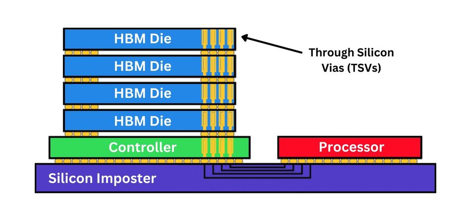
BRAM is used to store data buffers, FIFOs, and scratch memory for signal-processing algorithms. High‑end FPGAs also support high‑bandwidth memory (HBM) stacks to maximize memory bandwidth.
High‑Speed Transceivers
Dedicated transceiver blocks transmit and receive multi‑gigabit serial data without consuming core logic. They support protocols like PCIe, Ethernet and Serial RapidIO. Digilent explains that transceivers enable high‑speed data transfer to and from the FPGA [1]. Modern devices offer cutting‑edge connectivity; Versal Gen 2 by AMD supports PCIe Gen6 and CXL 3.1 interfaces.
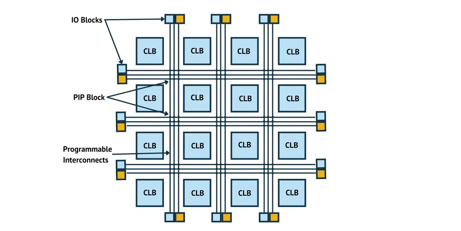
Input/Output Blocks (IOBs)
IOBs interface the FPGA fabric with external pins. They include programmable input and output buffers, level shifters and termination circuits. IOBs support a variety of single‑ended and differential signaling standards such as LVCMOS, LVTTL and LVDS [3], enabling compatibility with sensors, memories and communication interfaces. Transceivers provide multi‑gigabit capabilities, while IOBs handle lower‑speed general‑purpose I/O.
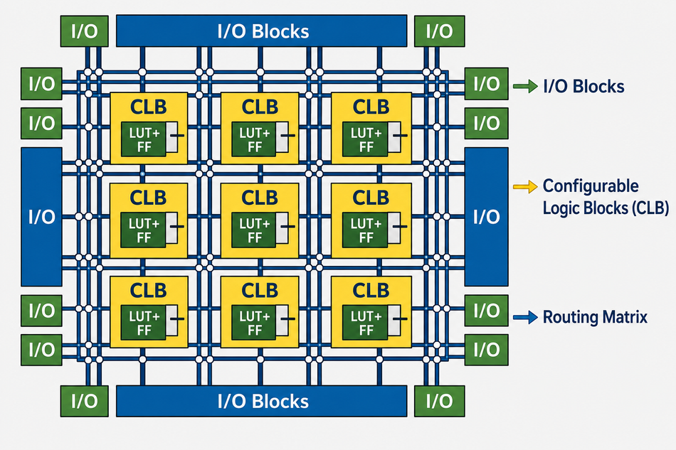
Programmable Interconnects and Routing
Programmable interconnect wires and switch matrices connect CLBs, DSP slices, BRAM and I/O. The routing network can occupy 80–90% of the silicon area in an FPGA [3].
Designers configure multiplexers and pass transistors within switch matrices to create custom signal paths. Routing resources include local lines for connections within a CLB, short and long lines for nearby blocks, and global lines for clock and reset distribution.
Clock Management Resources
FPGAs contain specialized clocking resources to distribute low‑skew clock signals. Modern devices provide global and regional clock networks, I/O clocks, and on‑chip frequency synthesizers such as Phase‑Locked Loops (PLLs) and Mixed‑Mode Clock Managers (MMCMs). These resources generate and manipulate clock frequencies, provide phase shifts and jitter filtering, and ensure synchronous operation across the device. Designers can also employ clock enables, clock multiplexers and dual‑clock FIFOs for clock domain crossing.
How Does an FPGA Work?
FPGA is a two‑dimensional array of configurable logic blocks (CLBs) connected by a programmable interconnect network. Each CLB contains multiple slices composed of look‑up tables (LUTs), flip‑flops and multiplexers. LUTs implement combinational logic by storing truth‑table values; flip‑flops and latches provide synchronous storage [4].
The dedicated carry logic accelerates arithmetic functions, while multiplexers and switch matrices route signals within and between slices. In AMD/Xilinx 7‑series devices, each CLB contains two slices - SLICEL and SLICEM; a SLICEL houses four 6‑input LUTs and eight flip‑flops, while a SLICEM can also function as distributed memory or a shift register [3].
Programming an FPGA involves writing HDL code that describes the desired circuit at a behavioral or register‑transfer level. The synthesis tools convert this description into a gate‑level netlist. Place‑and‑route algorithms then map the netlist onto physical CLBs, DSP slices, block RAM and routing resources, creating a configuration bitstream. Loading this bitstream configures the configuration memory of the device so that LUTs, flip‑flops and interconnects implement the specified logic. Because the bitstream can be changed at any time, the same silicon can implement different designs throughout its lifetime.
Unlike processors, which execute instructions sequentially, FPGAs operate as spatial architectures - operations are laid out in hardware and can run concurrently. Millions of adaptive logic modules (ALMs), tens of thousands of memory blocks and thousands of DSP blocks can execute in parallel [5]. Data flows through deeply pipelined hardware rather than being fetched and decoded by a control unit, reducing latency and improving energy efficiency. This capability to build custom pipelines makes FPGAs ideal for high‑throughput tasks such as real‑time signal processing, AI inference, and networking.
For a deeper examination of the overall fabric, see FPGA architecture. To learn about how fabrication technologies, process nodes and chip packaging affect device characteristics, see FPGA chip.
Modern FPGA Families and Process Nodes
The FPGA landscape evolves rapidly, as the recent product families push the boundaries of performance, power and integration:
| Vendor and Family | Process Node and Architecture | Key Features and Applications |
| AMD Versal Premium Series Gen 2 | Advanced TSMC FinFET adaptive SoC architecture for high-bandwidth acceleration. | PCIe Gen6, CXL 3.1, DDR5/LPDDR5X, high-speed transceivers; targets data centers, communications, aerospace, defense, and test systems. |
| AMD Versal AI Edge Series Gen 2 | Heterogeneous adaptive SoC architecture optimized for real-time edge AI workloads. | Next-generation AI Engines, embedded processing, programmable logic; used in ADAS, robotics, machine vision, medical imaging, and industrial automation. |
| AMD Versal Prime Series Gen 2 | Mainstream adaptive SoC platform combining programmable logic and Arm processors. | Balanced processing, connectivity, security, and safety features; suited for industrial control, embedded vision, robotics, and secure edge systems. |
| Intel/Altera Agilex 5 E-Series | Intel 7 process with second-generation Hyperflex FPGA architecture. | Arm Cortex-A76/A55 cores, AI tensor blocks, PCIe, Ethernet, transceivers; targets industrial automation, embedded vision, edge AI, and aerospace. |
| Lattice Nexus 2 | TSMC 16 nm FinFET platform optimized for low-power embedded FPGAs. | Low-power fabric, instant-on configuration, improved density, MIPI support; designed for IoT, sensors, portable electronics, and compact machine vision. |
| Lattice Avant Platform | 16 nm FinFET mid-range FPGA platform for low-power performance. | Higher capacity, 25 Gbps SERDES, PCIe, DSP resources; supports edge AI, embedded vision, industrial automation, and communications bridging. |
These FPGA families reflect three major directions in modern programmable logic development. AMD is expanding adaptive SoCs across high-bandwidth acceleration, real-time edge AI, and mainstream embedded computing. Intel/Altera is focusing on efficient midrange FPGAs with embedded Arm processors, AI tensor acceleration, and strong industrial and edge-computing capabilities. Lattice is strengthening both low-power and midrange FPGA segments, where instant-on operation, compact packaging, energy efficiency, embedded vision, and flexible connectivity are key design priorities.
Recommended Reading: Tensor Cores vs CUDA Cores: The Powerhouses of GPU Computing from Nvidia
Advantages of FPGAs
FPGAs offer several advantages over other technologies, including:
Flexibility: FPGAs can be reprogrammed to implement different functions, making them suitable for a wide range of applications.
Rapid Prototyping: FPGAs allow designers to quickly test and iterate on their designs, reducing time-to-market.
Parallelism: FPGAs can execute multiple tasks simultaneously, improving performance in certain applications.
Customization: FPGAs enable the creation of application-specific hardware tailored to meet specific requirements, often leading to optimized performance and reduced power consumption.
Reconfigurability: FPGAs can be reconfigured in the field, enabling updates, bug fixes, or feature additions without replacing the entire hardware.
Lower NRE Costs: FPGA development does not require the high non-recurring engineering (NRE) costs associated with custom ASIC designs, making them more affordable for small-scale productions or proof-of-concept projects.
Scalability: FPGA designs can be easily scaled up or down depending on the requirements, enabling efficient resource utilization and cost-effective solutions.
Security: FPGAs can provide increased security through hardware-based encryption and secure boot features, which are more difficult to tamper with compared to software-based implementations.
Analog and Digital Interfacing: FPGAs can interface with a wide variety of analog and digital peripherals, simplifying system integration and allowing seamless communication between different components.
Longevity: FPGA-based designs often have longer lifespans than ASICs, as they can be updated and reprogrammed to accommodate evolving standards and technologies.
Design Reuse: IP cores and previously developed FPGA designs can be easily reused and integrated into new projects, reducing development time and effort.
Disadvantages of FPGAs
FPGAs have a few disadvantages compared to other technologies, such as ASICs and microcontrollers. These include:
Cost: FPGAs can be more expensive than microcontrollers or ASICs, especially for high-volume production. The per-unit cost of an FPGA is generally higher than that of an ASIC or microcontroller for large quantities.
Power Consumption: FPGAs typically consume more power than ASICs and microcontrollers, which can be a concern in power-sensitive applications.
Design Complexity: The design process for FPGAs can be more complex than for microcontrollers, requiring specialized knowledge of hardware design, HDL, synthesis, and place-and-route tools.
Performance Limitations: Although FPGAs offer parallelism and can deliver high performance for some tasks, they may not be as fast as ASICs for certain applications, as ASICs are custom-designed for a specific purpose and can be highly optimized for performance.
Size: FPGAs can be larger than equivalent ASICs or microcontrollers, as they include additional resources for programmability and reconfiguration.
Configuration Time: FPGAs require configuration at startup, which can lead to longer startup times than ASICs and microcontrollers.
Recommended Reading: FPGA vs Microcontroller: Understanding the Key Differences and Use Cases
FPGA vs. ASIC vs. CPU/GPU vs. Microcontroller
To choose the right compute platform, engineers must weigh performance, flexibility, cost, power and development effort.
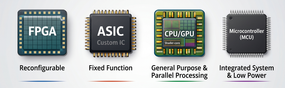
FPGA: Reconfigurable Hardware for Parallel Processing
FPGA is best suited for applications that require custom hardware behavior, deterministic latency, and parallel execution. Unlike a processor that executes instructions sequentially, an FPGA implements logic directly in hardware using configurable logic blocks, programmable routing, memory resources, DSP slices, and I/O blocks.
FPGAs are highly valuable when a design may need to change after deployment. Engineers can update the bitstream to modify functionality, add features, fix design issues, or optimize performance without replacing the physical device. This makes FPGAs ideal for prototyping, real-time DSP, edge AI, custom accelerators, communications systems, aerospace electronics, industrial control, and adaptable hardware platforms.
However, FPGAs usually consume more power and cost more per unit than ASICs in high-volume production. They also require specialized development skills, including HDL design, synthesis, simulation, placement, routing, and timing closure.
ASIC: Maximum Efficiency for Fixed Functions
ASIC is a custom silicon designed for one fixed function. Once fabricated, its hardware behavior cannot be changed. This makes ASICs less flexible than FPGAs, but far more efficient for mature, high-volume applications.
ASICs deliver the best performance, lowest power consumption, and smallest die area for a specific workload. They are commonly used in smartphones, networking chips, data-center accelerators, image processors, consumer electronics, and other products where the same function will be manufactured at scale.
The main drawback is development cost. ASICs require long design cycles, expensive verification, physical design, mask generation, fabrication, and testing. For this reason, they are only practical when the expected production volume justifies the high non-recurring engineering cost.
CPU/GPU: Software Flexibility and Mature Ecosystems
CPUs and GPUs are software-programmable platforms with fixed hardware architectures. CPU is optimized for general-purpose computing, control flow, operating systems, and scalar workloads. GPU is optimized for massively parallel data processing, graphics rendering, AI training, and SIMD-style workloads.
Compared with FPGAs, CPUs and GPUs are easier to program because they use mature software languages, libraries, compilers, and development frameworks. They are often the best choice when development speed, software flexibility, and ecosystem support are more important than deterministic latency or hardware-level optimization.
However, CPUs and GPUs execute workloads through predefined instruction sets. They cannot physically reshape their hardware datapaths like an FPGA. For streaming workloads, custom protocols, irregular data movement, or ultra-low-latency pipelines, an FPGA may offer better efficiency and timing control.
Microcontroller: Simple, Low-Cost Embedded Control
Microcontroller is a compact, low-power processor designed for embedded control tasks. It typically integrates a CPU core, memory, timers, communication peripherals, ADCs, GPIOs, and power-management features on a single chip.
Microcontrollers are ideal for simple control-oriented applications such as IoT devices, sensors, motor control, consumer appliances, basic automation, and battery-powered systems. They are inexpensive, easy to program, and supported by simple toolchains.
However, microcontrollers provide limited parallelism and lower computational throughput than FPGAs. They are not well suited for high-speed signal processing, custom digital interfaces, or hardware acceleration. In many embedded systems, a microcontroller handles control and communication while an FPGA manages real-time processing or custom logic.
Choosing Between Platforms
FPGAs vs. ASICs: Use FPGAs when flexibility, prototyping speed and upgradability outweigh per‑unit cost and peak efficiency. The application-specific integrated circuits (ASICs) suit high‑volume, performance‑critical products.
FPGAs vs. CPUs/GPUs: FPGAs provide deterministic latency and energy‑efficient parallelism for streaming tasks. CPUs and GPUs are better for software‑centric workloads or when rapid development is more important than efficiency. FPGAs are reconfigurable spatial architectures where operations execute concurrently in customized pipelines [5], whereas CPUs and GPUs are fixed architectures executing instructions sequentially or via SIMD [5].
FPGAs vs. Microcontrollers: Microcontrollers offer low‑cost, low‑power control for simple tasks and are easier to program. FPGAs handle computation‑intensive, real‑time tasks and custom digital protocols. FPGAs are reconfigurable hardware platforms while microcontrollers are fixed‑architecture processors designed for sequential software.
Recommended Reading: ASIC vs FPGA: A Comprehensive Comparison
FPGA Design Process and Methodology
In this section, we explore the FPGA design process, including design flow, hardware description languages, register-transfer level (RTL) design, synthesis, implementation, and testing and debugging.
Design Flow Overview
The FPGA design flow consists of several steps that guide designers from concept to a fully functional FPGA implementation. These steps include:
Design Entry: Designers create a high-level representation of the desired digital circuit using an HDL like VHDL or Verilog.
RTL Design and Simulation: The HDL code is translated into RTL, then simulated to verify functionality and performance.
Synthesis: The RTL design is converted into a gate-level netlist, a representation of the digital circuit using gates and flip-flops.
Implementation: The gate-level netlist is mapped to the resources of FPGA, including CLBs, DSP slices, and programmable interconnects. This step includes place-and-route and bitstream generation.
Testing and Debugging: FPGA devices are tested and debugged with simulation tools, testbenches, or target hardware to ensure correct functionality and performance.
Throughout the design flow, various tools and software are used to facilitate the design, simulation, synthesis, and implementation of FPGA designs.
RTL Design and Simulation
RTL design is an intermediate representation of a digital circuit that focuses on the flow of data between registers and the operations performed on that data. RTL simulation is used to verify the functionality and performance of the design before moving on to the synthesis and implementation stages.
The common RTL simulation tools include ModelSim, XSIM, and VCS. These tools allow designers to perform functional and timing simulations, which help identify and fix design errors and performance bottlenecks early in the design process.
Synthesis and Implementation
During the synthesis phase, the RTL design is converted into a gate-level netlist, which represents the digital circuit using gates and flip-flops. This process involves optimizing the design for area, speed, and power consumption. The common synthesis tools include Xilinx Vivado, Intel Quartus, and Synopsys Design Compiler. [6]
The implementation phase involves mapping the gate-level netlist to the resources of the FPGA, such as CLBs, DSP slices, and programmable interconnects. This step includes place-and-route, which determines the physical locations of the design elements on the FPGA, and bitstream generation, which creates the binary file that configures the FPGA.
The implementation tools include Xilinx Vivado and Intel Quartus. EDA (Electronic Design Automation) tools play a critical role in the FPGA design flow, assisting designers in all tasks, including synthesis, placement, routing, and verification.
Testing and Debugging FPGA Designs
Testing and debugging are crucial steps in the FPGA design process, ensuring that the design functions correctly and meets performance requirements. The common testing methods include:
Simulation: Using simulation tools to test the design in a virtual environment, allowing for faster and more controlled testing.
In-Circuit Testing: Testing the FPGA design on the testbench or target hardware, often using a logic analyzer or an oscilloscope to monitor signals and identify issues.
Debugging FPGA designs involves identifying and fixing issues related to functionality, performance, and resource usage. The best practices for debugging include:
Using descriptive signal and variable names to improve code readability.
Employing a modular design approach, breaking the design into smaller, more manageable components.
Leveraging simulation tools and in-circuit testing to identify and isolate issues.
By following the FPGA design flow and employing best practices for testing and debugging, designers can create high-quality FPGA designs that meet the requirements of their specific applications.
Recommended Reading: RTL Design: Comprehensive Guide to Understanding and Implementing Register-Transfer Level Design
FPGA Design Examples and Applications
In this section, we will explore various examples and applications of FPGA designs.
Digital Signal Processing (DSP) with FPGAs
DSP is the manipulation and analysis of digital signals, such as audio, video, or sensor data. FPGAs are well-suited for DSP tasks due to their parallelism and flexibility. Some examples of FPGA-based DSP applications include:
Audio Processing: FPGAs can be used for audio effects, equalization, noise reduction, and compression.
Image Processing: FPGAs can perform real-time image processing tasks like edge detection, filtering, and object recognition.
Software-Defined Radio (SDR): FPGAs can be used to implement various radio communication protocols, enabling highly customizable and adaptable radio systems.
FPGA-based Artificial Intelligence (AI) and Machine Learning (ML)
FPGAs play a significant role in AI and ML applications, offering advantages such as low latency, high throughput, and energy efficiency.
Some examples of FPGA-based machine learning and AI projects include:
Deep Learning Accelerators: FPGAs can accelerate deep neural network training and inference, improving performance and reducing power consumption compared to traditional CPU- and GPU-based solutions.
Edge AI: FPGAs enable AI processing at the edge, reducing the need to transmit data to the cloud and improving privacy and security.
Custom AI Hardware: FPGAs enable the implementation of custom AI algorithms tailored to specific applications, optimizing performance and power efficiency.
FPGAs in Networking and Communication
FPGAs are widely used in networking and communication systems, offering high performance, flexibility, and adaptability. Some examples of FPGA-based networking and communication projects include:
Network Switches and Routers: FPGAs can be used to implement high-performance, low-latency Ethernet switches and routers, enabling faster and more efficient data transmission.
Optical Communication: FPGAs can be used in optical communication systems, such as dense wavelength division multiplexing (DWDM), to implement high-speed data transmission and signal processing.
Wireless Communication: FPGAs can be used to implement various wireless communication protocols, such as 5G, Wi-Fi, and Bluetooth, enabling customizable and adaptable communication systems.
In summary, FPGAs are versatile and powerful devices that can be used in a wide range of applications where the capabilities of a microprocessor may be more than required. By leveraging the unique capabilities of FPGAs, designers can create innovative, high-performance solutions across various industries and use cases.
Recommended Reading: The 2026 Edge AI Technology Report
Best Practices for FPGA Design
In this section, we will discuss general best practices for FPGA design, focusing on code readability, modularity, and techniques to optimise performance, power, and resource usage.
Code Readability and Modularity
Maintaining code readability and modularity is crucial for efficient FPGA design. By following these practices, you can improve the maintainability and scalability of your designs:
Descriptive Naming: Use meaningful names for signals, variables, and modules to make your code more understandable.
Comments: Include comments to explain the purpose and functionality of your code, especially for complex or non-obvious operations.
Modularity: Break your design into smaller, more manageable modules or components. This approach makes it easier to debug, maintain, and reuse code.
Optimizing FPGA Designs for Performance, Power, and Resource Usage
Optimizing your FPGA design can help you achieve the desired balance between performance, power consumption, and resource usage. Some optimization techniques include:
Pipelining: Break complex operations into smaller stages and process them in parallel to increase throughput and reduce latency.
Resource Sharing: Reuse hardware resources, such as multipliers, converters or memory blocks, for multiple operations to save area and power.
Clock Gating: Disable the clock domain signal to unused or idle portions of your design to reduce dynamic power consumption.
By following best practices for FPGA design and employing optimization techniques, you can create high-quality, efficient designs that meet the needs of your specific applications.
Recommended Reading: The Ultimate Guide to ASIC Design: From Concept to Production
Conclusion
Field‑programmable gate arrays occupy a unique position in the spectrum of computing hardware. They enable engineers to build custom digital circuits in reconfigurable silicon, combining the flexibility of software with the determinism of hardware. The advances in process technology and device architecture have expanded the FPGA landscape to encompass edge AI, data‑center acceleration and ultra‑low‑power IoT nodes. By understanding FPGA architecture, components, design flow and best practices, engineers can harness these devices for applications that demand high performance, low latency and adaptability. Selecting among FPGAs, ASICs, CPUs/GPUs, and microcontrollers ultimately depends on the application requirements for performance, power, cost, and flexibility. FPGAs provide an invaluable middle ground where custom hardware and rapid iteration intersect.
Frequently Asked Questions (FAQs)
Q. How is an FPGA different from an ASIC?
A. ASICs are custom‑designed for a fixed function and deliver maximum performance and efficiency, but they require long development cycles and high non‑recurring engineering costs. FPGAs are reconfigurable; designers can implement and modify digital circuits after manufacture and reuse the same device for multiple projects.
Q. What languages are used to program FPGAs?
A. FPGAs are commonly programmed using hardware description languages such as Verilog and VHDL. These languages describe logic gates, registers, interconnects, and programmable logic blocks. Engineers also use high-level synthesis tools, Python-based frameworks, and vendor tutorials for faster development.
Q. Can FPGAs run software like processors?
A. FPGAs do not run software directly like CPUs. They implement hardware circuitry using look-up tables, flip-flops, and routing resources. However, designers can add soft-core processors or use adaptive SoCs that combine FPGA fabric with hard processor cores.
Q. What types of memory are used in FPGAs?
A. FPGAs use several memory types, including distributed RAM, block RAM, external DDR memory, and sometimes high-bandwidth memory. Many FPGAs rely on SRAM configuration cells, which store the bitstream that defines programmable connections and logic behavior.
Q. Are FPGAs suitable for AI applications?
A. Yes. FPGAs are suitable for AI inference because they provide low latency, parallel pipelines, and efficient custom arithmetic. Their programmable logic blocks, DSP slices, memory resources, and I/O blocks support edge AI, vision systems, and high performance computing workloads.
Q. Can FPGAs replace microcontrollers in embedded systems?
A. FPGAs can replace microcontrollers when applications require parallel processing, custom interfaces, or precise timing. However, microcontrollers are simpler for control tasks. Many embedded systems combine both, using FPGAs to connect external devices and accelerate time-critical functions.
References
[1] Digilent. What is an FPGA? Uses, Applications & Advantages [Cited 2026 May 28]; Available at: Link
[2] Fortune Business Insights. Field Programmable Gate Array Market Size, Share & Industry Analysis [Cited 2026 May 28]; Available at: Link
[3] Wevolver. FPGA Architecture: A Comprehensive Guide for Digital Design Engineers [Cited 2026 May 28]; Available at: Link
[4] Digilent. FPGA – Configurable Logic Block [Cited 2026 May 28]; Available at: Link
[5] Intel. Compare Benefits of CPUs, GPUs, and FPGAs for Different oneAPI Compute Workloads [Cited 2026 May 28]; Available at: Link
[6] Wevolver. Comprehensive Guide to FPGA Development Boards [Cited 2026 May 28]; Available at: Link
in this article
1. Key Takeaways2. Introduction3. Understanding FPGA Basics4. How Does an FPGA Work?5. Modern FPGA Families and Process Nodes6. Advantages of FPGAs7. Disadvantages of FPGAsFPGA vs. ASIC vs. CPU/GPU vs. Microcontroller9. FPGA Design Process and Methodology10. FPGA Design Examples and Applications11. Best Practices for FPGA Design12. Conclusion13. Frequently Asked Questions (FAQs)14. References