Semiconductor Fabrication Process: The Ultimate Guide to Creating Cutting-Edge Electronics
Semiconductors have become an integral part of our modern lives that relies heavily on electronics, serving as the foundation for a wide range of such devices, from smartphones and computers to medical equipment, automotive applications, and renewable energy systems.

18 Apr, 2023. 21 minutes read
Introduction
As technology continues to evolve at a rapid pace, understanding the process of semiconductor fabrication, abbreviated as “fab”, becomes increasingly important for anyone working in or interested in the field of electronics. In this article, we will briefly explain what a semiconductor is and its role in modern technology. We will also touch on the importance of understanding the semiconductor fabrication process and introduce the purpose of this guide.
1. Fundamentals of Semiconductors
Before diving into the complex world of semiconductor fabrication, it is essential to have a solid understanding of the basic properties of semiconductors.
Semiconductors are those materials whose conductivity and resistivity lie between conductors and insulators. In general, a semiconductor is a device that allows current flow for an applied voltage. The energy gap in a semiconductor material is between conductors and insulators, approximately 2-3 eV. These unique electrical properties make them ideal for use in a wide range of electronic devices. In this section, we will explore the main types of semiconductors, the process of doping, and the various materials commonly used in the fabrication of semiconductor devices.
1.1. Types of Semiconductors
Semiconductors can be broadly classified into two main categories: intrinsic and extrinsic. Intrinsic semiconductors are pure materials that have a balanced number of majority and minority charge carriers, resulting in a relatively low electrical conductivity. On the other hand, extrinsic semiconductors are created by introducing impurities, or dopants, into the intrinsic material, which significantly alters its electrical properties.
Doping is the process of adding impurities to a semiconductor material to create either n-type or p-type semiconductors. N-type semiconductors are created by introducing donor impurities that provide additional free electrons, increasing the material's conductivity. Conversely, p-type semiconductors are formed by adding acceptor impurities that create additional holes, making the material more conductive to positive charges.
Both n-type and p-type semiconductors have unique properties and applications, with each playing a critical role in the formation of electronic devices. For example, the combination of n-type and p-type materials can be used to create diodes, transistors, thyristors, amplifiers, and other fundamental components of modern electronics.
2.2. Semiconductor Materials
While a wide range of materials can exhibit semiconductor properties, some materials are more commonly used in the fabrication of electronic devices due to their specific characteristics. Two of the most prevalent semiconductor materials are silicon and gallium arsenide.
Silicon is the most widely used semiconductor material, primarily due to its abundance, low cost, and relatively stable properties at high temperatures. The electric conductivity of Silicon is around 1000 S/m. Additionally, silicon has a well-established fabrication infrastructure, making it an attractive choice for manufacturers. However, silicon does have some drawbacks, such as lower electron mobility compared to other materials, which can limit the performance of high-speed devices.
Gallium arsenide is another popular semiconductor material, valued for its higher electron mobility and direct bandgap. These properties make it well-suited for optoelectronic applications, such as lasers and solar cells. However, gallium arsenide is more expensive and less abundant than silicon, which can limit its widespread adoption. Another drawback of gallium arsenide is that exists intrinsically as a semi-insulator rather than a semiconductor with an electrical conductivity of 0.000001 S/m.
Aside from silicon and gallium arsenide, researchers are continually exploring new materials with promising semiconductor properties. These materials include aluminium nitride, carbon nanotubes, and many other materials that have the potential to revolutionize the industry. As our understanding of these emerging materials grows, it is likely that they will play an increasingly important role in the future of semiconductor fabrication.
2. Semiconductor Fabrication Process Overview
The semiconductor fabrication process is a complex and highly specialized series of steps that transform raw materials into functional electronic components. This process involves a multitude of techniques and technologies, with each stage requiring precise control and attention to detail. In this section, we will provide an overview of the various stages involved in semiconductor fabrication, from the growth of the semiconductor crystal to the final packaging of the device.
2.1. Crystal Growth and Wafer Preparation
The fabrication process begins with the growth of a high-quality semiconductor crystal, which serves as the base material for the production of electronic devices. In the case of silicon, the most common method for crystal growth is the Czochralski process. Other widely used processes include the Kyropoulos method, the Floating Zone technique, the Verneuil method, the Bridgman technique, etc. The Czochralski process involves melting high-purity silicon under a controlled atmosphere and then cooling it to zero degrees Celsius. Then a single crystal is extracted from the melt and sliced into thin film wafers. Furthermore, the wafers are carefully polished and cleaned to create a pristine surface for subsequent processing steps. One of the benefits of using the Czochralski process is that it yields good growth of the crystals.
Recommended Readings: Microcontroller Programming- Mastering the Foundation of embedded systems
2.2. Photolithography and Patterning
Photolithography is a crucial optical process in the fabrication process, as it is used to create intricate circuit patterns on a single wafer's surface. This is achieved by coating the wafer with a photosensitive material, called a photoresist, and then exposing it to high-wavelength deep ultraviolet (DUV) or extreme ultraviolet (EUV) light through a mask containing the desired pattern. The exposed photoresist undergoes a chemical change, which allows it to be selectively removed. It leaves behind a patterned layer that serves as a protective layer for subsequent processing steps, such as etching and deposition.
2.3. Etching and Deposition
Etching and deposition are two essential processes that enable the creation of the various layers and structures that make up a semiconductor device. Etching involves the selective removal of material from the wafer, either through a wet chemical process or a dry plasma process. This allows for the creation of complex three-dimensional structures, such as transistors and interconnects.
Deposition, on the other hand, is the process of adding thin layers of material onto the wafer's surface. There are several deposition techniques, such as chemical vapour deposition (CVD) and physical vapour deposition (PVD), which can be used to deposit a wide range of materials, including metals, insulators, and semiconductors.
2.4. Doping and Ion Implantation
Doping and ion implantation are crucial steps in the fabrication process, as they allow for the creation of n-type and p-type semiconductor regions within the device. Doping involves the introduction of impurities, or dopants, into the semiconductor material, which significantly alters its electrical properties. These impurities include the introduction of trivalent or pentavalent impurities. Injection of the diffusion layer, heating semiconductor material, and ion implantation are common methods of introducing dopant atoms. Ion implantation is the most common doping technique that involves bombarding the wafer with a beam of ions. Further, these ions are embedded in the semiconductor material, creating the desired n-type or p-type regions.
2.5. Metallization and Interconnects
Metallization is the process of depositing metal layers onto the wafer's surface, which serves as electrical connections between the various components of the device. Post-creation of p-type or n-type regions, the process of metallization ensures electrical connections through a conductive in between the internal circuitry. These metal layers can be deposited using a variety of techniques, such as sputtering or CVD. The metal layers are then patterned and etched to form the desired interconnect structures.
2.6. Passivation and Packaging
Passivation involves the deposition of a protective layer of silicon nitride or oxide layer like silicon dioxide, onto the wafer's surface. This layer serves to protect the delicate underlying structures from damage and contamination during the packaging process and subsequent use.
Packaging is the final stage of the fabrication process, in which the completed wafer is diced into individual chips. Each chip is then mounted, interconnected, and encapsulated in a protective housing. This packaging serves to protect the chip from physical damage, as well as to provide electrical connections between the semiconductor device and the external circuitry.
In conclusion, the semiconductor fabrication process is a highly intricate and specialized series of steps that involve a wide range of techniques and technologies. From the initial crystal growth and wafer preparation to the final packaging of the device, each stage requires careful attention to detail and precise control to ensure the production of high-quality, reliable electronic components. As technology continues to advance, it is likely that the semiconductor fabrication process will continue to evolve, enabling the creation of increasingly complex and powerful devices that will drive the future of the electronics industry.
3. Wafer Preparation
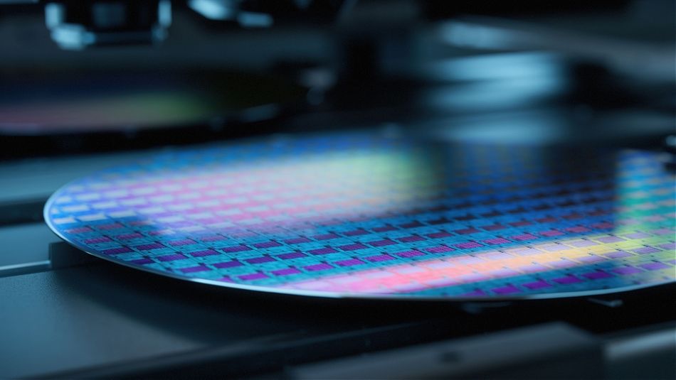
Wafer preparation is a critical initial step in the semiconductor fabrication process, as it lays the foundation for creating high-quality electronic devices. The process involves transforming a semiconductor crystal, such as silicon or gallium arsenide, into a thin-flat wafer with an extremely smooth surface. This section will delve into the various stages of wafer preparation, including crystal growth, wafer slicing, polishing, and cleaning.
3.1. Crystal Growth
Crystal growth is the process of producing a large, high-quality semiconductor crystal, which serves as the starting material for wafer production. For silicon-based devices, the most common method of crystal growth is the Czochralski process, which involves melting high-purity silicon in a crucible and cooling it to a temperature near the freezing point. Then the process allows for pulling a single crystal out of the melt using a rotating seed crystal. This method produces a monocrystalline ingot, which has a uniform crystal structure and excellent electrical properties.
Other methods for crystal growth include the Bridgman-Stockbarger method, which involves slowly cooling a molten semiconductor material in a controlled environment. The Float Zone method is another method particularly useful for producing very high-purity silicon crystals.
3.2. Wafer Slicing
Once a semiconductor crystal has been grown, it is then sliced into thin wafers using a process known as wafer slicing or wafering. Depending upon the wafer size, the process of slicing involves either wires or blades. This is typically accomplished using a wire saw, which cuts the crystal ingot into wafers of uniform thickness, usually ranging from a few hundred micrometres to over a millimetre. The wafers are then carefully inspected to ensure they are free of defects and meet the required specifications.
3.3. Polishing
After slicing, the wafers undergo a series of polishing steps to create a smooth, mirror-like surface. This is important because any surface imperfections or contaminants can adversely affect the performance and reliability of the final semiconductor devices. The polishing process typically involves a combination of chemical and mechanical techniques, such as chemical-mechanical planarization (CMP). The process uses a slurry containing abrasive particles and a chemical reactant to remove material from the wafer surface in a controlled manner.
3.4. Cleaning
Following polishing, the wafers must be thoroughly cleaned to remove any residual particles, contaminants, or chemical residues. This is usually accomplished using a combination of wet and dry cleaning techniques like ultrasonic and plasma cleaning. Ultrasonic cleaning involves immersing the wafer in a cleaning solution and subjecting it to ultrasonic vibrations. On the other hand, plasma cleaning uses high-energy plasma to remove contaminants from the wafer surface.
In conclusion, wafer preparation is a critical step in the semiconductor fabrication process, as it lays the groundwork for creating high-quality electronic devices. By carefully controlling the crystal growth, wafer slicing, polishing, and cleaning processes, manufacturers can ensure that their wafers meet the stringent requirements necessary for the production of reliable, high-performance semiconductor devices.
4. Photolithography
Photolithography is a vital step in the semiconductor fabrication process, as it enables the creation of intricate patterns of circuitry on the surface of a wafer. These patterns form the foundation for the various components and structures that make up a semiconductor device. In this section, we will discuss the key elements of the photolithography process, including photoresist application, mask alignment, exposure, and development.
4.1. Photoresist Application
Before the photolithography process begins, the wafer must be coated with a thin layer of a photosensitive material known as a photoresist. The photoresist is typically applied using a spin coating process, in which the wafer is spun at high speed while a small amount of photoresist is deposited onto its surface. The centrifugal force ensures that the photoresist spreads out evenly, resulting in a uniform coating. The basic function of a photoresist coating is to lose resistance upon being subject to chemical processes and create patterns.
There are two main types of photoresists: positive and negative. Positive photoresists become more soluble when exposed to light, while negative photoresists become less soluble. The choice of photoresist depends on the specific requirements of the semiconductor device being fabricated.
4.2. Mask Alignment
After the photoresist has been applied, a photomask is used to transfer the desired pattern onto the wafer. A photomask is a glass or quartz plate with a patterned layer of an opaque material, such as chrome, that blocks light transmission. The wafer and photomask are carefully aligned using a specialized tool called a mask aligner or stepper, which ensures that the pattern is accurately positioned on the wafer surface.
4.3. Exposure
With the photomask in place, the wafer is exposed to ultraviolet (UV) light that passes through the transparent regions of the photomask and strikes the photoresist. The UV light triggers a chemical reaction in the exposed regions of the photoresist, altering its solubility. In the case of positive photoresists, the exposed areas become more soluble, while for negative photoresists, they become less soluble.
The exposure process can be carried out using various light sources, such as mercury-vapour lamps or excimer lasers. They can be further refined using techniques like immersion lithography, which involves immersing the wafer and photomask in a liquid medium to enhance the resolution of the pattern transfer.
4.4. Development
After exposure, the wafer is immersed in a developer solution that selectively removes the soluble regions of the photoresist to reveal the patterned layer beneath. For positive photoresists, the exposed areas are removed and for negative photoresists, the unexposed areas are removed. The wafer is then rinsed and dried, leaving behind a precisely patterned photoresist layer that serves as a template for subsequent fabrication steps, such as etching or deposition.
In summary, photolithography is a crucial step in the semiconductor fabrication process, to enable the creation of complex patterns and structures on the wafer surface. By carefully controlling the photoresist application, mask alignment, exposure, and development processes, manufacturers can achieve high-resolution pattern transfer, which is essential for the production of advanced semiconductor devices.
Recommended Readings: 3D printing: large complex marine superstructures
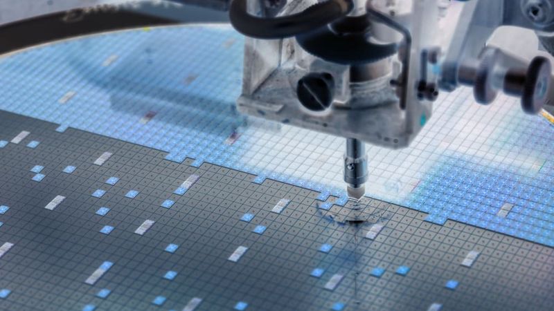
5. Etching
Etching is an essential step in the semiconductor fabrication process that involves the selective removal of material from the wafer to create the desired structures and features. This process is used to define the shapes of various components, such as transistors, capacitors, and interconnects, by removing the unmasked regions of the wafer. The desired region of the wafer is protected using a photoresist and the undesired portion is removed. In this section, we will discuss the key aspects of etching, including wet etching, dry etching, and the importance of etch selectivity and uniformity.
5.1. Wet Etching
Wet etching is a chemical process that involves immersing the wafer in a liquid etchant solution, which reacts with the exposed material to dissolve and remove it. The choice of etchant depends on the material being etched and the desired etch rate and selectivity. Wet etching is generally isotropic, meaning it removes material uniformly in all directions, which can result in the undercutting of features and limits the resolution of the etched structures.
5.2. Dry Etching
Dry etching is a gas-phase process that uses chemically reactive or physically energetic species to remove material from the wafer surface. There are several types of dry etching techniques, including:
Reactive Ion Etching (RIE): Reactive ion etching uses a combination of chemical reactions and ion bombardment to etch the material. The wafer is placed in a vacuum chamber and exposed to plasma generated from a reactive gas mixture. The reactive species in the plasma react with the exposed material, while the ions accelerate towards the wafer and physically remove the reaction products.
Deep Reactive Ion Etching (DRIE): DRIE is a variation of RIE specifically designed for the high-aspect-ratio etching of silicon. It utilizes alternating deposition and etching steps to achieve deep, vertical trenches with smooth sidewalls.
Atomic Layer Etching (ALE): ALE is an advanced etching technique that enables the removal of material one atomic layer at a time. This is achieved through sequential self-limiting reactions, which provide exceptional control over the etch depth and profile.
Dry etching techniques offer better control over the etch profile compared to wet etching. Furthermore, dry etching techniques can achieve anisotropic etching to remove material preferentially in a specific direction and enable the creation of high-resolution, vertical structures.
5.3. Etch Selectivity and Uniformity
Etch selectivity refers to the ability of an etching process to selectively remove one material while leaving another material unaffected. High etch selectivity is critical for preserving the integrity of the masked regions of the wafer and preventing damage to the underlying layers. Etch uniformity, on the other hand, refers to the evenness of the etching process across the entire wafer surface, which is important for ensuring consistent device performance.
In conclusion, etching is a fundamental step in the semiconductor fabrication process that enables the creation of intricate structures and features on the wafer surface. By carefully selecting the appropriate etching techniques and maintaining high etch selectivity and uniformity, manufacturers can produce advanced semiconductor devices with high performance and reliability.
6. Doping and Ion Implantation
Doping is a critical process in semiconductor fabrication that involves the intentional introduction of impurities, known as dopants, into the semiconductor material to modify its electrical properties. Dopants can create either an excess of free electrons (n-type doping) or a deficiency of electrons, known as holes (p-type doping), which are essential for the formation of semiconductor devices like transistors and diodes. Some n-type pentavalent impurities include Phosphorus, Antimony, and Arsenic. On the other hand, Boron, Aluminium, Gallium, and Indium are some examples of trivalent p-type impurities. In this section, we will discuss the main techniques used for doping, including ion implantation and diffusion, as well as the importance of precise doping control.
Recommended Readings: Zener Diode: A Comprehensive Guide to Its Principles and Applications
6.1. Ion Implantation
Ion implantation is a widely used doping technique that involves the direct insertion of dopant ions into the semiconductor material. The process involves ionizing the desired dopant species, accelerating the ions using an electric field, and directing them toward the wafer surface. The high-energy ions penetrate the wafer and become embedded in the crystal lattice, altering the electrical properties of the material.
Ion implantation offers several advantages over other doping techniques, including:
Precise control over the dopant concentration and depth
Uniform dopant distribution across the wafer surface
Low-temperature processing, which reduces the risk of damage to the wafer
However, ion implantation can also cause damage to the crystal lattice, which must be repaired through a subsequent annealing process.
6.2. Diffusion
Diffusion is another common doping technique that relies on the movement of dopant atoms through the semiconductor material at elevated temperatures. In this process, the wafer is placed in a controlled environment, such as a diffusion furnace, and exposed to a source of dopant atoms. The dopant atoms diffuse into the wafer, creating a concentration gradient that determines the electrical properties of the material.
Diffusion offers several benefits, including the ability to form shallow junctions and the simultaneous doping of multiple wafers. However, it is generally less precise than ion implantation and can result in non-uniform dopant distribution across the wafer surface.
6.3. Precise Doping Control
Accurate control of the doping process is crucial for achieving the desired electrical properties and performance characteristics of semiconductor devices. Factors such as dopant concentration, distribution, and junction depth can have a significant impact on device characteristics like threshold voltage, current-carrying capacity, and switching speed. As a result, manufacturers must carefully control the doping process to ensure that devices meet stringent performance and reliability requirements.
In conclusion, doping is a fundamental process in semiconductor fabrication that enables the creation of semiconductor devices with tailored electrical properties. By carefully selecting the appropriate doping techniques, such as ion implantation or diffusion, and maintaining precise control over the doping process, manufacturers can produce high-performance semiconductor devices that meet the demanding requirements of modern electronic applications.
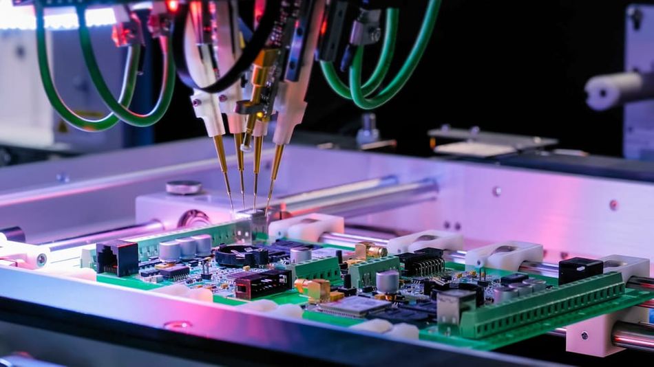
7. Metallization and Interconnects
Metallization and interconnects are crucial components of semiconductor devices, providing the electrical pathways that connect the various elements of the integrated circuit. These connections enable the transfer of electrical signals and power between transistors, resistors, capacitors, and other components on the wafer. In this section, we will discuss the key aspects of metallization and interconnects, including material selection, deposition techniques, and the challenges associated with scaling and performance.
7.1. Material Selection
The choice of materials for metallization and interconnects is critical, as it directly impacts the performance and reliability of the semiconductor device. Common materials used for interconnects include aluminium, copper, and tungsten, which offer a combination of low resistivity, good adhesion, and compatibility with the underlying semiconductor material.
In recent years, copper has become the material of choice for many advanced semiconductor devices, due to its lower resistivity and higher electromigration resistance compared to aluminium. However, copper also presents several challenges, such as the potential for diffusion into the surrounding materials, which must be carefully managed through the use of barrier layers and dielectric materials.
7.2. Deposition Techniques
Deposition techniques play a critical role in the formation of metallization layers and interconnect on the wafer surface. There are several common deposition methods used in the semiconductor industry, including:
Physical Vapor Deposition (PVD): PVD techniques, such as sputtering and evaporation, involve the transfer of material from a solid or liquid source onto the wafer surface through the application of energy, such as heat or ion bombardment.
Chemical Vapor Deposition (CVD): CVD techniques involve the formation of a solid material on the wafer surface through a chemical reaction between gaseous precursors. CVD methods offer excellent step coverage and uniformity, making them well-suited for the deposition of conformal layers and the filling of narrow trenches and vias.
Electrochemical Deposition (ECD): ECD, also known as electroplating, is a technique used primarily for the deposition of copper interconnects. It involves the reduction of metal ions from a solution onto the wafer surface through the application of an electric current.
Each deposition technique has its advantages and limitations. The choice of method depends on factors such as the material being deposited, the desired film properties, and the specific requirements of the semiconductor device.
7.3. Scaling and Performance Challenges
As semiconductor devices continue to scale down in size, metallization and interconnects become increasingly critical to devise performance and reliability. Shrinking feature sizes result in increased resistance and capacitance, leading to higher power consumption, signal delays, and potential reliability issues, such as electromigration and stress-induced voiding. However, the reduced size of a chip has been an interesting trend in the electronics industry for a long time. According to Moore’s law, the transistor number on a chip doubles every two years. With the such reduction, semiconductors have now reached those small sizes that deal with quantum effects such as tunnelling. In this effect, a low-energy particle can cross the barrier potential below the threshold voltage.
To address these challenges, researchers are exploring new materials, such as graphene and carbon nanotubes that might offer the potential for improved electrical performance and reduced power consumption. Additionally, advances in deposition techniques and the use of low-k dielectric materials are helping to mitigate the impact of scaling on interconnect performance.
In summary, metallization and interconnects are essential components of semiconductor devices, providing the electrical connections that enable the transfer of signals and power between the various elements of the integrated circuit. By carefully selecting the appropriate materials, and deposition techniques, and addressing the challenges associated with scaling, manufacturers can continue to push the boundaries of semiconductor device performance and integration.
8. Passivation and Packaging
Passivation and packaging are essential final steps in the semiconductor fabrication process that serve to protect the delicate integrated circuitry from external factors, such as moisture, contaminants, and mechanical stress. In this section, we will discuss the importance of passivation and packaging, the materials and techniques used, and the challenges associated with these processes as semiconductor devices continue to scale down in size.
8.1. Passivation
Passivation involves the application of a thin, protective layer of insulating material on the surface of the wafer to shield the semiconductor devices from environmental factors and reduce the risk of corrosion, contamination, and electrical leakage. Common passivation materials include silicon dioxide (SiO2), silicon nitride (Si3N4), and polyimide, which offer good adhesion, low moisture permeability, and compatibility with the underlying semiconductor materials.
There are several techniques used for passivation layer deposition, such as:
Chemical Vapor Deposition (CVD)
Plasma-Enhanced Chemical Vapor Deposition (PECVD)
Spin Coating
Each technique has its advantages and limitations, with the choice of the method depending on factors such as the desired film properties, the specific requirements of the semiconductor device, and the compatibility with the underlying materials.
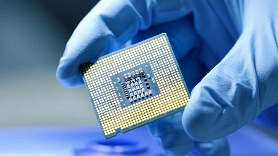
8.2. Packaging
Packaging is the process of enclosing the semiconductor die in a protective casing to provide mechanical support, thermal management, and electrical connections to the external environment. The packaging process typically involves several steps, including:
Die singulation: Cutting the individual dies from the wafer
Die bonding: Attaching the die to a substrate or lead frame
Wire bonding or flip-chip bonding: Connecting the die's electrical contacts to the package leads
Encapsulation: Sealing the die and interconnections in a protective material, such as epoxy or ceramic
There are various types of semiconductor packages, including:
Dual In-line Package (DIP)
Quad Flat Package (QFP)
Ball Grid Array (BGA)
Chip Scale Package (CSP)
The choice of package type depends on factors such as the device's electrical, thermal, and mechanical requirements, as well as cost and chip manufacturing considerations.
8.3. Challenges in Passivation and Packaging
As semiconductor devices continue to scale down in size and increase in complexity, the challenges associated with passivation and packaging become more pronounced. Some of these challenges include:
Thinner passivation layers: As devices shrink, the thickness of the passivation layer must also decrease, which can compromise its protective properties and make it more susceptible to defects.
Increased thermal management requirements: Smaller devices often generate more heat, necessitating improved thermal management solutions within the package design.
High-density interconnects: The need for more interconnects in smaller packages requires the development of advanced interconnect technologies, such as through-silicon vias (TSVs) and micro-bumps.
To address these challenges, researchers are exploring new materials and technologies. 3D packaging is a technique that involves the stacking of multiple semiconductor dies to achieve higher levels of integration and performance.
In conclusion, passivation and packaging are critical final steps in the semiconductor fabrication process that serve to protect the delicate integrated circuitry and enable reliable, high-performance operation. By carefully selecting the appropriate materials and techniques, and addressing the challenges associated with scaling, manufacturers can continue to advance the state of the art in semiconductor device technology.
9. Testing and Quality Control
Testing and quality control are essential aspects of the semiconductor fabrication process to ensure that the final product meets performance and reliability specifications. These processes involve various inspection, measurement, and evaluation techniques to identify and correct defects, improve process control, and maintain high manufacturing yields. In this section, we will discuss the key aspects of testing and quality control in semiconductor fabrication, including wafer inspection, electrical testing, and reliability assessment.
9.1. Wafer Inspection
Wafer inspection is a critical step in the fabrication process to identify defects, such as particles, scratches, and pattern irregularities, that can impact device performance and yield. There are several inspection techniques used in the semiconductor industry, including:
Optical inspection: Involves the use of high-resolution imaging systems and specialized software to identify defects on the wafer surface.
Scanning Electron Microscopy (SEM): Provides high-resolution imaging of the wafer surface by scanning it with a focused electron beam.
Atomic Force Microscopy (AFM): Measures the surface topography of the wafer by scanning a sharp probe over the surface, providing detailed information about surface roughness and defects.
These inspection techniques enable early detection and correction of defects, helping to maintain high manufacturing yields and minimize the risk of producing faulty devices.
9.2. Electrical Testing
Electrical testing is performed at various stages of the semiconductor fabrication process to evaluate the performance and functionality of the devices. Some common electrical testing methods include:
Parametric testing: Involves the measurement of key electrical parameters, such as voltage, current, and resistance, to ensure that the devices meet performance specifications.
Functional testing: Tests the functionality of the integrated circuit under specific operating conditions, such as temperature and voltage, to ensure proper operation.
Burn-in testing: Involves the operation of the devices under accelerated stress conditions, such as elevated temperatures and voltages, to identify potential reliability issues and weed out early failures.
These testing methods help to ensure that the final semiconductor devices meet their performance and reliability requirements and are suitable for use in their intended applications.
9.3. Reliability Assessment
Reliability assessment is an ongoing process throughout the semiconductor fabrication process, aimed at evaluating and improving the long-term performance and stability of the devices. Some common techniques used for reliability assessment include:
Accelerated life testing: Involves the operation of devices under extreme stress conditions, such as high temperature, humidity, and voltage, to identify potential failure mechanisms and estimate their lifetimes.
Failure analysis: Involves the systematic investigation of failed devices to identify the root causes of failure and implement corrective actions to improve the manufacturing process and device reliability.
Statistical process control: Involves monitoring and analysing manufacturing data to identify trends, variations, and potential process issues, enabling continuous improvement of the fabrication process.
By implementing comprehensive testing and quality control processes, semiconductor manufacturers can ensure that their devices meet the stringent performance and reliability requirements of today's demanding applications while driving continuous improvement in manufacturing efficiency and yield.
In summary, testing and quality control are essential aspects of the semiconductor fabrication process, helping to ensure that the final devices meet performance and reliability specifications, maintain high manufacturing yields, and minimize the risk of producing faulty products. By employing a combination of inspection, measurement, and evaluation techniques, manufacturers can continue to advance the state of the art in semiconductor device technology and maintain their competitive edge in the global market.
Conclusion
The semiconductor fabrication process is a complex and intricate series of steps that transform raw materials into highly advanced integrated circuits. This process involves numerous critical stages, including wafer preparation, photolithography, etching, doping, metallization, passivation, packaging, and testing. With ongoing advances in materials, techniques, and equipment, the semiconductor industry continues to push the boundaries of innovation and scale, enabling the development of ever-smaller, more powerful, and more efficient electronic devices.
In this article, we have provided a comprehensive overview of the semiconductor fabrication process, focusing on the key aspects of each stage, the challenges faced by manufacturers, and the strategies employed to overcome these challenges. By understanding the fundamental principles and technologies behind semiconductor fabrication, we can appreciate the incredible feats of engineering and ingenuity that have driven the rapid progress of the electronics industry and enabled the digital revolution that has transformed our world.
FAQs about the Semiconductor Manufacturing process
Q1: What is a semiconductor?
A: A semiconductor is a material that has electrical conductivity properties between those of conductors (like metals) and insulators (like glass). Semiconductors are widely used in electronic devices due to their ability to control the flow of electrical current through the manipulation of impurities and the application of electric fields.
Q2: Why are silicon wafers used in semiconductor fabrication?
A: Silicon wafers are the most common substrate material used in semiconductor fabrication due to their excellent electrical properties, abundant availability, electrical conductivity and relatively low cost. Silicon is also highly compatible with various fabrication processes and can be easily doped with impurities to modify its electrical characteristics.
Q3: What is the role of photolithography in semiconductor fabrication?
A: Photolithography enables the transfer of patterns into a wafer through a mask. It is a critical step in the semiconductor fabrication process that involves the transfer of intricate patterns onto the wafer surface using light-sensitive chemicals and ultraviolet light. This process enables the precise patterning of the various layers that make up the integrated circuit, including the transistors, interconnects, and other components.
Q4: What are the main challenges associated with scaling down semiconductor devices?
A: As semiconductor devices continue to scale down in size, manufacturers face several challenges, including the need for more advanced patterning techniques, thinner layers, and higher-density interconnects. Additionally, smaller devices often generate more heat, necessitating improved thermal management solutions within the package design.
Q5: How is quality control maintained in the semiconductor fabrication process?
A: Quality control is maintained through a combination of inspection, measurement, and evaluation techniques, including wafer inspection, electrical testing, and reliability assessment. These processes help to identify and correct defects, improve process control, and maintain high manufacturing yields to ensure that the final semiconductor devices meet their performance and reliability requirements.
References
https://aip.scitation.org/doi/10.1063/1.5133039
https://dspace.mit.edu/bitstream/handle/1721.1/46221/41494616-MIT.pdf?sequence=2
https://ieeexplore.ieee.org/document/6570490
https://en.wikipedia.org/wiki/Semiconductor_device_fabrication
https://www.sciencedirect.com/topics/engineering/semiconductor-manufacturing
in this article
1.1. Types of Semiconductors2.2. Semiconductor Materials2.1. Crystal Growth and Wafer Preparation2.2. Photolithography and Patterning2.3. Etching and Deposition2.4. Doping and Ion Implantation2.5. Metallization and Interconnects2.6. Passivation and Packaging3.1. Crystal Growth3.2. Wafer Slicing3.3. Polishing3.4. Cleaning13. References