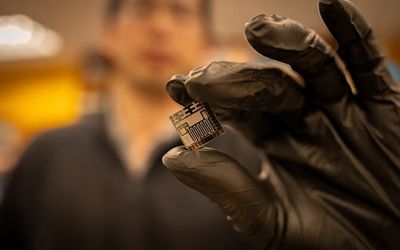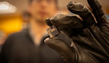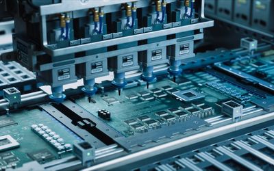

Featured
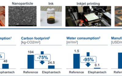
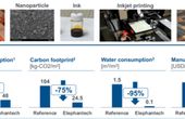
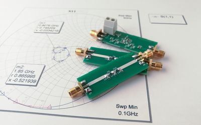
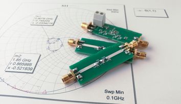
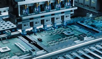
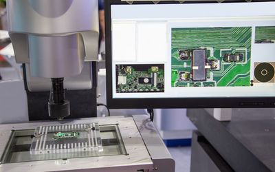
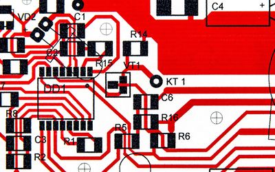
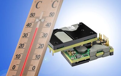
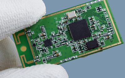
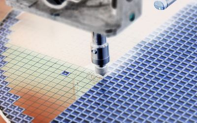
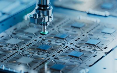
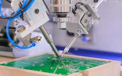
Additive electronics is sustainable reduceing copper and water consumption vs. the traditional PCB production processes by 70% and 95%, respectively whilst reducing the carbon footprint by 75%. Here you will read about the latest advances by one of the leading firms in the field from Japan