Featured
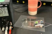
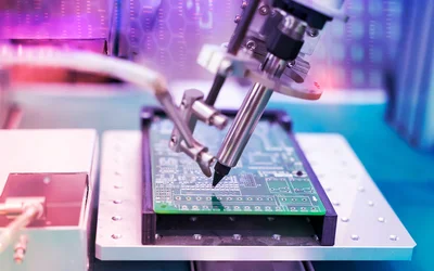
Duru Uluk, a Voltera test engineering intern, created an induction mug heater using in-mold electronics (also known as in-mold structural electronics).
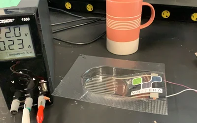
Duru Uluk, a Voltera test engineering intern, created an induction mug heater using in-mold electronics (also known as in-mold structural electronics).
PCB Trace Width Calculator
Glossary of Semiconductors Terms
Duru Uluk, a Voltera test engineering intern, created an induction mug heater using in-mold electronics (also known as in-mold structural electronics).
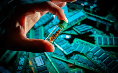
A new method safely extracts valuable metals locked up in discarded electronics and low-grade ore using dramatically less energy and fewer chemical materials than current methods, report University of Illinois Urbana-Champaign researchers in the journal Nature Chemical Engineering.
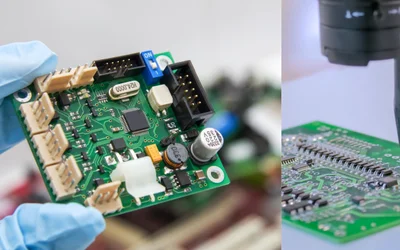
Hackers can access sensitive data and disrupt device operations by activating embedded malware or hardware trojans in counterfeit components. How can you avoid these issues?
Semiconductors are the building blocks of modern electronics, powering everything from smartphones to satellites. This in-depth guide provides a comprehensive understanding of semiconductors' engineering principles and applications, delving into their fundamental concepts, materials, devices, manufacturing processes, and their impact on today's technology landscape.
13 minutes read.
13 minutes read.
20 minutes read.
16 minutes read.
20 minutes read.
20 minutes read.


Semiconductors
Nordic Semiconductor is a fabless semiconductor company specializing in wireless technology that powers the IoT.
181 Posts
A guide covering the full radio-frequency design workflow, starting from setting specifications and choosing topologies to matching, simulation, layout, and verification, to help antenna engineers.
This article presents a detailed technical exploration of SiC MOSFET devices, covering material physics, device structure, switching behavior, and practical design considerations for high-efficiency power electronics systems.
This article is a comprehensive technical guide to relay wiring diagrams, covering 4-pin and 5-pin configurations, working principles, safety practices, standards, and advanced relay applications in modern systems.
Explore how frequency shapes EMC behavior from RF emissions to ultra-low-frequency drift, with mitigation strategies for robust, compliant electronic system design.
How Essentra Components Supports Engineering from Concept to Production
Makera gives live demonstrations of the Z1 during the 2026 Hackaday Europe event. The Z1 is a compact CNC manufacturing platform.
A crystal oscillator is an electronic circuit that uses a quartz crystal to produce a precise and stable frequency reference. This article covers crystal operation, equivalent circuit models, resonance, load capacitance, oscillator topologies, stability, aging, and design practices.
June 25, 2026 at 08:00 PM Central European Summer Time
Duru Uluk, a Voltera test engineering intern, created an induction mug heater using in-mold electronics (also known as in-mold structural electronics).

5 minutes read
A new method safely extracts valuable metals locked up in discarded electronics and low-grade ore using dramatically less energy and fewer chemical materials than current methods, report University of Illinois Urbana-Champaign researchers in the journal Nature Chemical Engineering.

2 minutes read
Hackers can access sensitive data and disrupt device operations by activating embedded malware or hardware trojans in counterfeit components. How can you avoid these issues?

7 minutes read
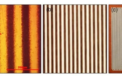
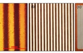
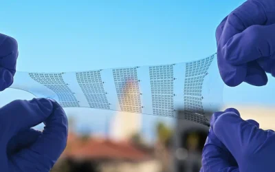
R2R Sputtering + Direct Laser Patterning is a great way to create large-area circuits on flexible circuits, even with materials such as graphene or MoS2. The technology R2R produces high-quality uniform films on large substrates whilst the laser forms precision circuit patterns without photolith.

2 minutes read
This comprehensive series delves into the fundamentals of PCB design, including design workflow, signal integrity, manufacturing, testing and debugging, advanced design techniques, and the latest software and tools available for PCB design.
This comprehensive series delves into the fundamentals of PCB design, including design workflow, signal integrity, manufacturing, testing and debugging, advanced design techniques, and the latest software and tools available for PCB design.
Multi-material printing without inks? The technology’s on-demand and in-situ nanoparticle generation and real-time sintering capability allow the printing of various electronics and functional devices with pure, multifunctional, hybrid materials printing - without inks and with bulk properties!
3 minutes read
Adequate component spacing is typically not high on the PCB designer's list of priorities, but oversights can be frustrating and could demand substantial re-work. Here we look at an example, give general guidelines and look at how tools can be used to educate designers and save time.

6 minutes read
The world is witnessing a rise in more electric aircraft (MEA) where only the propulsion remains fuel-driven and other subsystems are electric rather than hydraulic or pneumatic. Find out what this change means for EEs.
5 minutes read
Engineers, researchers, entrepreneurs, inventors, and end users are invited to join TechBlick Innovations Festival, exploring additive, printed, 3D, and wearable electronics on 25 April 2024 online.
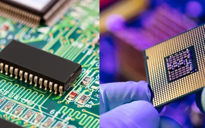
This article provides a detailed understanding of microprocessor vs integrated circuit, their basics, key differences, future trends, challenges, and how they synergize to form the backbone of our digital systems.
Artificial intelligence (AI) is providing an opportunity for the electronics industry to accelerate design and development and speed up part sourcing.
Stanford researchers have developed soft integrated circuits that are powerful enough to drive a micro-LED screen and small enough to read thousands of sensors in a single square centimeter.

4 minutes read
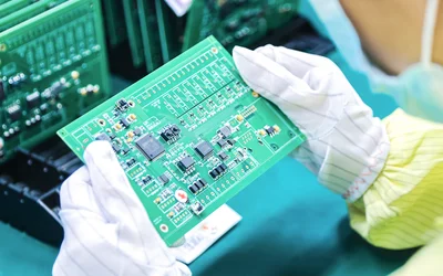
Understanding circuit board components is essential. It's key to creating and fixing gadgets in our tech-filled world. In this article, we’ll explore popular circuit board components and various techniques to identify them.
Parker and Stephen chat with James Lewis (aka the Bald Engineer) about constructing a functional computer based on the Apple II GS's Mega II chip, and also announce a contest sponsored by Mouser!
3 minutes read