Featured
This guide explores the crucial factors in capacitor polarity, its mathematical analysis, identification, and advanced practices for improved circuit performance.
This guide explores the crucial factors in capacitor polarity, its mathematical analysis, identification, and advanced practices for improved circuit performance.
PCB Trace Width Calculator
Glossary of Semiconductors Terms
This guide explores the crucial factors in capacitor polarity, its mathematical analysis, identification, and advanced practices for improved circuit performance.
Explore the different types of solder, their unique properties, and their critical roles in various engineering applications. Understand how to choose the right solder for your project and the considerations involved.
Autonomous robotics must anticipate and plan for the unexpected, often in harsh, changing environments. We take a deep dive into these challenges by exploring design considerations beyond those associated with conventional PCBAs.
Semiconductors are the building blocks of modern electronics, powering everything from smartphones to satellites. This in-depth guide provides a comprehensive understanding of semiconductors' engineering principles and applications, delving into their fundamental concepts, materials, devices, manufacturing processes, and their impact on today's technology landscape.
13 minutes read.
13 minutes read.
20 minutes read.
16 minutes read.
20 minutes read.
20 minutes read.


Semiconductors
Nordic Semiconductor is a fabless semiconductor company specializing in wireless technology that powers the IoT.
181 Posts
A guide covering the full radio-frequency design workflow, starting from setting specifications and choosing topologies to matching, simulation, layout, and verification, to help antenna engineers.
This article presents a detailed technical exploration of SiC MOSFET devices, covering material physics, device structure, switching behavior, and practical design considerations for high-efficiency power electronics systems.
This article is a comprehensive technical guide to relay wiring diagrams, covering 4-pin and 5-pin configurations, working principles, safety practices, standards, and advanced relay applications in modern systems.
Explore how frequency shapes EMC behavior from RF emissions to ultra-low-frequency drift, with mitigation strategies for robust, compliant electronic system design.
How Essentra Components Supports Engineering from Concept to Production
Makera gives live demonstrations of the Z1 during the 2026 Hackaday Europe event. The Z1 is a compact CNC manufacturing platform.
A crystal oscillator is an electronic circuit that uses a quartz crystal to produce a precise and stable frequency reference. This article covers crystal operation, equivalent circuit models, resonance, load capacitance, oscillator topologies, stability, aging, and design practices.
June 25, 2026 at 08:00 PM Central European Summer Time
This guide explores the crucial factors in capacitor polarity, its mathematical analysis, identification, and advanced practices for improved circuit performance.
Explore the different types of solder, their unique properties, and their critical roles in various engineering applications. Understand how to choose the right solder for your project and the considerations involved.
Autonomous robotics must anticipate and plan for the unexpected, often in harsh, changing environments. We take a deep dive into these challenges by exploring design considerations beyond those associated with conventional PCBAs.

6 minutes read
This article delves into the fundamentals of EMI gaskets, types, and their critical role in protecting electronic devices and ensuring optimal performance in various engineering applications.
Wevolver was present at the recent Embedded World event in Nuremberg to launch the 2024 Edge AI report.
Silicon Carbide (SiC) wafers are specialized materials employed in semiconductor technology, crafted from silicon carbide. This article explores the advent of silicon carbide (SiC) wafers and how it has opened up new possibilities in power electronics.
Discover the science behind EMI shielding and its crucial role in ensuring the reliability and performance of electronic devices across various industries.
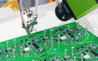
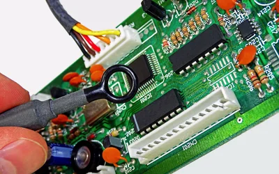
This article delves into the various types of printed circuit boards, their fundamental concepts, structures, manufacturing processes, and advanced PCB technologies, highlighting their advantages, limitations, and typical applications.
EPFL researchers are targeting the next generation of soft actuators and robots with an elastomer-based ink for 3D printing objects with locally changing mechanical properties, eliminating the need for cumbersome mechanical joints.

3 minutes read
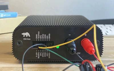
Discover the Qoitech Otii Arc Pro, the ultimate power analysis tool for enhancing device energy efficiency. Learn how its precision, user-friendly interface, and unique battery optimization features can transform your electronic design and development projects for the better.
Explore the transformative potential of the ROCK 3 Compute Module in revolutionizing pipeline inspection. Discover the power and versatility of this innovative solution, designed to enhance safety, efficiency, and operational excellence in infrastructure maintenance.
To excel in the fast-paced electronics industry, you need not just adaptability, but a cultivated expertise to discern the far-reaching impact of your design decisions. This eBook is your key to building such expertise.
5 minutes read
Are you an EE looking for a new podcast? Here's a list of MacroFab Circuit Break episodes to get you started.
12 minutes read
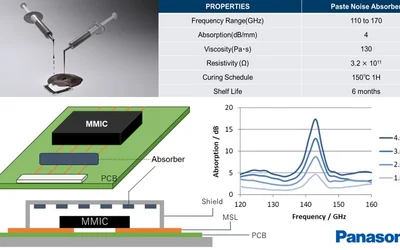
Properties and application of paste technology for noise reduction in high frequency (110-170 GHz) electronic devices and packaging . This is a dispensable material can be easily installed in narrow spaces, suppressing noise inside electronic devices used in beyond 5G/6G

Transitioning from Lab-scale in Printed Electronics: Going from lab and pilot equipment to rotary screen printing. Learn about example applications in printed low-power displays for use in retail as well as cost-per unit calculation comparing flat-bed vs. rotary screen printing for mass production
3 minutes read