Understanding the ENIG Finish: A Comprehensive Guide
This article delves into the basics of ENIG finish, its application process, advantages and disadvantages, challenges, and comparative analysis with other finishes.

31 Oct, 2023. 16 minutes read
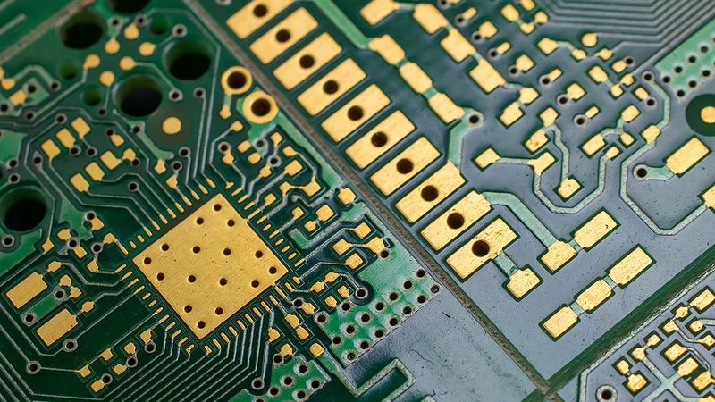
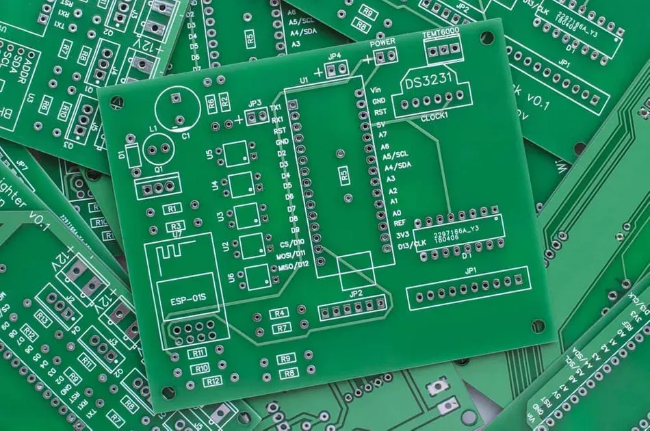
Printed Circuit Board with Electroless Nickel Immersion Gold; Credits: sfxpcb
Introduction
In the world of electronics, The ENIG finish, or Electroless Nickel Immersion Gold, is a critical aspect, particularly in Printed Circuit Board (PCB) manufacturing. This type of finish is applied to the copper surface of a PCB to protect it from oxidation and to prepare it for subsequent soldering of components.
The ENIG finish is important because it provides a reliable and robust surface for soldering, which is essential for the performance and longevity of electronic devices. It is especially favoured for its excellent surface planarity, making it suitable for PCBs with fine-pitch components, and its compatibility with lead-free soldering processes, which are becoming increasingly common due to environmental regulations.
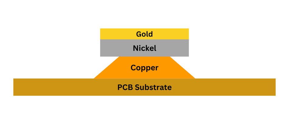
The ENIG finish is a two-layer metallic coating where the first layer, Electroless Nickel, acts as a barrier to the PCB base material and a durable surface for soldering. The second layer, Immersion Gold, protects the nickel during storage and provides low-contact resistance. The end result is RoHS (Restriction of Hazardous Substances) compliant. So, when discussing PCB manufacturing, ENIG finish holds prime importance in the process.
Basics of Electroless Nickel Immersion Gold (ENIG)
Electroless Nickel Immersion Gold (ENIG) is a type of surface plating used for printed circuit boards (PCBs). It consists of an electroless nickel plating covered with a thin layer of immersion gold, which protects the nickel from oxidation.
ENIG has several advantages over more conventional surface platings such as HASL (hot air solder levelling), including excellent surface planarity (flatness) and its suitability for fine-pitch components. The process of applying ENIG is complex and requires a series of chemical and cleaning stages.
The ENIG process, which can be quite complex, involves multiple stages, including cleaning the copper surface, activating the surface to accept the nickel plating, and depositing the nickel layer. Finally, the nickel-plated surface is immersed in a gold-containing solution to form the gold layer.
The Electroless Nickel Layer
The electroless nickel layer in ENIG serves a dual purpose. Firstly, it acts as a barrier layer between the copper substrate of the PCB and the solder used to mount components to the board. This is crucial because copper, when exposed to heat and air, can oxidize and degrade, leading to poor solderability and potential failure of the PCB.
Secondly, the nickel layer provides a robust and solderable surface for the mounting of electronic components. Unlike copper, nickel can withstand the high temperatures of the soldering process without substantial oxidation, ensuring a reliable electrical connection between the components and the PCB.
The electroless nickel plating process involves several steps. The PCB is first cleaned and micro-etched to prepare the copper surface for plating. The board is then immersed in a bath of nickel-phosphorus alloy, which deposits a nickel layer onto the copper surface. The thickness of the nickel layer is typically between 3-7 micrometres, which provides a good balance between cost, performance, and reliability. [1]
The nickel deposition process is autocatalytic, meaning that it occurs without the need for an external power source. A chemical reducing agent and deposit reduce the nickel ions in the bath onto the copper surface. The phosphorus in the bath is co-deposited with the nickel, resulting in a nickel-phosphorus alloy layer. The phosphorus content can vary between 2-14%, with higher phosphorus content resulting in a more corrosion-resistant layer. [2]
The nickel layer's quality and thickness are critical to the performance of the ENIG finish. Too thin a nickel layer can lead to problems such as nickel corrosion and solder joint failure, while too thick a layer can lead to issues such as brittle solder joints. Therefore, carefully controlling the plating process is essential to ensure a high-quality ENIG finish.
The Immersion Gold Layer
The immersion gold layer in ENIG serves a protective function. It is a thin layer of gold deposited over the nickel layer. The gold layer also provides a low-resistance electrical contact for the final assembly process.
The immersion gold process is a displacement reaction where the gold ions in the immersion bath displace the nickel atoms at the surface of the nickel layer. This process is self-limiting, meaning that once a complete monolayer of gold atoms has formed on the nickel surface, the reaction stops. This results in a very thin and uniform gold layer, typically 0.05-0.23 micrometres thick. [3]
The nickel-plated PCB is immersed in a bath containing gold ions, typically in the form of a gold cyanide complex. The gold ions displace the nickel atoms at the surface, forming a thin layer of gold. The PCB is then rinsed and dried to complete the process.
The quality of the gold layer is critical to the performance of the ENIG finish. A thin or discontinuous gold layer can lead to nickel oxidation and poor solderability. On the other hand, a gold layer that is too thick can lead to issues such as gold embrittlement of the solder joints. Therefore, like the nickel layer, careful control of the immersion gold process is essential to ensure a high-quality ENIG finish.
The immersion gold layer, despite its thinness, plays a crucial role in the performance and reliability of the ENIG finish. It protects the nickel layer from oxidation, provides a low-resistance electrical contact, and gives the PCB a pleasing golden appearance. Understanding the role of the immersion gold layer and its process is essential for anyone involved in PCB manufacturing or procurement.
Recommended Reading: PCB Surface Finish: The Ultimate Guide to Understanding and Choosing the Right Option
The ENIG Process
The process of applying the ENIG finish begins with the preparation of the copper surface of the PCB, followed by the deposition of the nickel and gold layers.
It starts with cleaning the PCB's copper surface to remove impurities. Next, this surface is activated with an electroless palladium catalyst, prepping it for the nickel layer. The board is then dipped in a nickel-phosphorus bath, where a chemical reaction deposits nickel onto the copper layer.
Following the nickel deposition, the PCB is rinsed and then immersed in a gold-containing bath. Here, gold ions replace some nickel atoms, creating a gold layer. The thickness of this layer is controlled by bath temperature and immersion duration. Finally, the PCB is rinsed, dried, and checked to ensure the ENIG finish's quality.
Pre-treatment
Pre-treatment is a critical step in the ENIG process. It involves preparing the copper surface of the PCB to accept the nickel plating. This is typically done using a series of chemical cleaning and micro-etching steps.
The cleaning step involves immersing the PCB in a cleaning solution to remove oxides or contaminants from the copper surface. This is typically done using an alkaline cleaner, which can effectively remove organic contaminants and oxides from the copper surface.
The micro-etching step involves immersing the PCB in an etching solution to roughen the copper surface. This increases the surface area of the copper, which helps to improve the adhesion of the nickel layer. The etching solution typically contains a strong acid and an oxidizing agent.
The pre-treatment process is critical to the success of the ENIG process. A poorly prepared copper surface can lead to poor adhesion of the nickel layer, resulting in a poor-quality ENIG finish. Therefore, careful control and monitoring of the pre-treatment process are essential to ensure a high-quality ENIG finish.
Nickel Deposition
Nickel deposition is a diffusion barrier surface finish that involves the accumulation of nickel onto a surface. This process can be achieved through various methods, each with unique mechanisms and applications.
Electroplating is one method used for nickel deposition. It involves using an electric current to reduce dissolved metal cations, enabling them to form a coherent metal coating on an electrode. In nickel deposition, a nickel salt solution serves as the electrolyte, providing the nickel cations. The object to be plated, such as a metal surface, acts as the cathode where the reduction of nickel cations occurs. This results in the deposition of a layer of nickel onto the surface. The thickness of the nickel layer can be controlled by adjusting the plating time and the electric current.
Electroless Plating is another method used for nickel deposition. Unlike electroplating, electroless plating does not require an external electric current. Instead, it relies on a chemical reduction to deposit nickel onto a surface. A nickel salt solution and a reducing agent are used in this process. The reducing agent reacts with the nickel ions in the solution, causing them to deposit onto the surface as a metallic nickel layer. Electroless plating can provide a uniform and continuous coverage of the surface, even in the presence of complex geometries.
Chemical Vapor Deposition (CVD) is used for depositing nickel as a thin film. In this process, a nickel precursor is heated to produce nickel-containing vapour. This vapour then reacts with the surface of the substrate, resulting in the deposition of a thin film of nickel. The deposition rate, which determines the thickness of the nickel layer, can be controlled by adjusting the temperature and the concentration of the nickel precursor.
| Characteristics | Electroplating | Electroless Plating | Chemical Vapour Deposition |
| Deposit Mechanism | Electrochemical | Autocatalytic | Chemical Vapor Reaction |
| Uses Electric Current | Yes | No | No |
| Thickness Control | Good | Fair | Excellent |
| Deposition Rate | Fast | Slow | Medium |
| Cost | Less | Normal | High |
Each of these methods has its advantages and limitations. Electroplating is simple and cost-effective, but not for non-conductive surfaces. Electroless plating and CVD can deposit nickel on a wider range of substrates but require more complex equipment and higher temperatures. Therefore, the choice of method depends on the specific requirements of the application.
Gold Deposition
Gold deposition is a process that involves the accumulation of gold onto a surface. This process can be achieved through various methods, each with unique mechanisms and applications. [4]
Electroplating is one such method. It involves using an electric current to reduce dissolved metal cations, enabling them to form a coherent metal coating on an electrode. In gold deposition, gold salt solution serves as the electrolyte, providing the gold cations. The object to be plated, such as a metal surface, acts as the cathode where the reduction of gold cations occurs. This results in the deposition of a layer of gold onto the surface. The thickness of the layer can be controlled by adjusting the gold plating time and the electric current.
Chemical Vapor Deposition (CVD) is another method used for gold deposition. In this process, a gold precursor is heated to produce gold-containing vapour. This vapour then reacts with the surface of the substrate, resulting in the deposition of a thin film of gold. The deposition rate, which determines the thickness of the gold layer, can be controlled by adjusting the temperature and the concentration of the gold precursor.
Thermal Evaporation is a physical vapour deposition process that can also be used for gold deposition. In this method, gold is heated in a vacuum until it evaporates. The gold vapour then condenses on the cooler surface of the substrate, forming a thin film of gold. The gold thickness can be controlled by adjusting the evaporation time and the temperature.
| Characteristics | Electroplating | Chemical Vapor Deposition | Thermal Evaporation |
| Deposit Mechanism | Electrochemical | Autocatalytic | Physical |
| Deposition Rate | Slow | Moderate | Fast |
| Film Thickness | Uniform | Uniform | Uniform |
| Cost | Less | High | Normal |
Each of these methods has its advantages and limitations. For instance, electroplating is relatively simple and cost-effective, but it may not be suitable for depositing gold onto non-conductive surfaces. On the other hand, CVD and thermal evaporation can deposit gold onto a broader range of substrates, but they require more complex equipment and higher operating temperatures. Therefore, the choice of method depends on the specific requirements of the application.
Advantages of ENIG finish
One of the primary benefits of ENIG is its excellent surface planarity. This makes it particularly suitable for PCBs with fine-pitch components, where the flatness of the surface is critical for ensuring good electrical contact. The uniformity of the ENIG finish also contributes to its excellent solderability, allowing for reliable solder joints. [5]
Another advantage of ENIG is its compatibility with both lead and lead-free solders. This versatility makes it a suitable choice for various applications, from consumer electronics to aerospace and defence systems. The end result is RoHS compliant, which makes this finish more important.
ENIG also provides a robust barrier against oxidation. The nickel layer acts as a barrier to prevent copper from the PCB from oxidizing, while the thin layer of gold protects the nickel from oxidation. This dual layer of protection enhances the longevity of the PCB, making ENIG a good choice for applications where durability is important.
Durability and Longevity
The ENIG finish is renowned for its durability and longevity, two of its standout features. The nickel layer in ENIG provides a hard and wear-resistant surface that can withstand mechanical stress. This makes ENIG-finished PCBs ideal for through holes, vias, connectors or Ball Grid Arrays (BGA) used in harsh environments. This PCB surface finish has a long shelf life of 12+ months.
The gold layer, although thin, provides excellent protection against corrosion. Gold is highly resistant to oxidation and tarnish, which helps to maintain the electrical performance of the PCB over time. This is particularly important in applications where the PCB is exposed to harsh environments, such as industrial or outdoor applications.
Furthermore, the electroless deposition process used in ENIG ensures a uniform and continuous coverage of the PCB surface, even in the presence of complex geometries. This uniform coverage further enhances the durability and longevity of the PCB by ensuring that all areas of the PCB surface are adequately protected.
In terms of longevity, ENIG-finished PCBs can maintain their performance for many years, even under challenging conditions. This long lifespan makes ENIG a cost-effective choice in the long run, despite its higher upfront cost than other surface finishes. ENIG is also a good surface finish for high-volume manufacturing, which is common in China.
Superior Performance
One of the key performance advantages of ENIG is its exceptional electrical conductivity. The gold layer in ENIG provides a highly conductive surface, which is crucial for the efficient operation of electronic devices. This high conductivity ensures minimal signal loss, particularly in high-frequency applications.
Another performance advantage of ENIG is its excellent thermal stability. The nickel layer in ENIG has a high melting point, which allows ENIG-finished PCBs to withstand high temperatures during soldering and operation. This thermal stability is critical in applications where the PCBs are exposed to high temperatures, such as in power electronics.
ENIG also offers superior performance in terms of surface flatness. The electroless deposition process ensures a uniform and flat surface, essential for the reliable assembly of fine-pitch components. This surface flatness contributes to the high yield and reliability of ENIG-finished PCBs.
Furthermore, ENIG provides excellent wetting properties, which facilitate the formation of reliable solder joints. This is particularly important in surface mount technology (SMT), where the quality of the solder joints directly affects the performance and reliability of the assembled devices.
Compatibility
In terms of compatibility, ENIG is compatible with a wide range of materials and processes. It can be used with both lead and lead-free solders, and it is compatible with various types of solder pastes and fluxes. This compatibility makes ENIG a versatile choice that can meet the diverse requirements of different applications.
The nickel layer in ENIG provides excellent corrosion protection, making it ideal for PCBs in challenging environments. ENIG's surface is highly conductive and easy to bond, making it perfect for wire bonding. It also provides a smooth surface for chip-scale packages (CSPs) and other applications that require a smooth finish. ENIG can withstand multiple reflow cycles, making it a top choice for projects that require frequent assembly.
Overall, the superior performance of ENIG in terms of electrical conductivity, thermal stability, surface flatness, wetting properties, and compatibility contributes to its widespread use in the electronics industry.
Disadvantages and Challenges of ENIG finish
While the Electroless Nickel Immersion Gold finish offers numerous advantages, it also has certain disadvantages and challenges that must be considered when selecting a surface finish for printed circuit boards (PCBs).
Cost Implications
One of the primary drawbacks of ENIG is its higher cost than other surface finishes, such as HASL (Hot Air Solder Leveling) or OSP (Organic Solderability Preservative). The ENIG process involves the deposition of both nickel and gold layers, which contributes to the increased cost. Additionally, the chemicals used in the electroless deposition process can be expensive, further driving up the overall cost of the finish.
The higher cost of ENIG may not be justified for all applications, particularly for low-cost consumer electronics or projects with tight budget constraints. In such cases, more cost-effective surface finishes may be preferred. ENIG is more expensive and more complex to apply than immersion tin.
However, it is essential to weigh the cost implications against the performance benefits and durability offered by ENIG. In some cases, the long-term benefits of using ENIG, such as improved reliability and longevity, may outweigh the initial cost difference. This is especially true for high-performance applications or those requiring a high level of reliability and durability.
Black Pad Phenomenon
Another challenge with ENIG is the potential for "black pad" syndrome, a defect that can occur during electroless nickel deposition. This defect is characterized by a brittle, non-uniform nickel layer, which can lead to poor solder joint reliability and potential failure of the PCB. [6] This issue occurs during the electroless nickel deposition process and can lead to poor solder joint reliability and potential failure of the printed circuitry.
The root cause of the black pad phenomenon is often attributed to the presence of contaminants or impurities in the electroless nickel plating bath, as well as inadequate process control during the deposition process.
To mitigate the risk of black pad syndrome, several measures can be taken:
Strict process control: Ensuring that the electroless nickel plating bath is maintained within the specified operating parameters, such as temperature, pH, and concentration of chemicals, is crucial for preventing black pad formation. Regular monitoring and adjustments of the plating bath can help maintain optimal conditions for the deposition process.
Bath maintenance: Regularly replenishing the plating bath with fresh chemicals and removing contaminants can help maintain the quality of the nickel layer. This includes filtering the bath to remove particulate matter and monitoring the concentration of metal ions to ensure that they remain within the specified limits.
Surface preparation: Properly cleaning and preparing the copper surface before the deposition process can help reduce the risk of black pad formation. This may involve using appropriate cleaning agents and rinsing procedures to remove residual contaminants from the copper surface.
Quality control: Implementing rigorous quality control measures, such as visual inspection and solderability testing, can help identify and address black pad issues before the PCBs are assembled and deployed.
By taking these precautions and maintaining strict process control, the risk of the black pad phenomenon can be minimised, ensuring the reliability and performance of ENIG-finished PCBs.
In summary, while ENIG offers several advantages in terms of performance, durability, and compatibility, it also comes with certain disadvantages and challenges, such as higher cost and the potential for black pad syndrome. These factors should be carefully considered when selecting a surface finish for PCBs.
Comparing ENIG with Other Finishes
Let’s compare the Electroless Nickel Immersion Gold (ENIG) finish with other common finishes, such as Hot Air Solder Leveling (HASL), Organic Solderability Preservative (OSP), and Immersion Silver (ImAg). [7]
Hot Air Solder Leveling (HASL) is a widely used and cost-effective surface finish. It involves applying molten solder to the PCB surface and levelling it using hot air knives. HASL provides good solderability and is compatible with both lead and lead-free solders. However, HASL has some drawbacks compared to ENIG. The surface planarity of lead-free HASL is not as good as ENIG, which can be problematic for fine-pitch components. Additionally, HASL may not be suitable for high-frequency applications due to its higher signal loss compared to ENIG.
Organic Solderability Preservative (OSP) is another surface finish option that provides a thin, protective layer on the exposed copper surface of the PCB. OSP is cost-effective and offers good surface planarity. However, OSP has a limited shelf life and may not provide the same level of protection against oxidation as ENIG. Furthermore, OSP is not as robust as ENIG in terms of durability and may not be suitable for applications requiring high reliability and longevity.
Immersion Silver (ImAg) is a surface finish that involves depositing a thin layer of silver onto the PCB surface. ImAg offers good solderability and surface planarity, similar to ENIG. However, ImAg is more susceptible to tarnishing and oxidation than ENIG, which can affect its long-term performance. Additionally, ImAg may require more stringent storage and handling conditions to maintain its performance characteristics.
ENIG offers superior performance in terms of surface planarity, durability, and compatibility with various materials and processes. However, it comes with a higher cost and potential challenges like the black pad phenomenon. Other finishes, such as HASL, OSP, and ImAg, may be more cost-effective but may not provide the same level of performance and protection as ENIG.
Recommended Reading: HASL vs ENIG Surface Finishes: Understanding the Difference
Conclusion
Electroless Nickel Immersion Gold (ENIG) is a widely used surface finish for printed circuit boards (PCBs) due to its numerous advantages, such as excellent surface planarity, compatibility with various materials and processes, and superior performance in terms of electrical conductivity, thermal stability, and solderability. However, ENIG has some disadvantages and challenges, including higher costs and the potential for the black pad phenomenon.
When selecting a surface finish for PCBs, it is essential to consider the specific requirements of the application and weigh the advantages and disadvantages of various finishes, such as Hot Air Solder Leveling (HASL), Organic Solderability Preservative (OSP), and Immersion Silver (ImAg). Each finish has its unique characteristics, and the choice depends on factors such as cost, performance, durability, and compatibility with the intended application.
FAQs
Q: What is the primary advantage of ENIG over other surface finishes?
A: The primary advantage of ENIG is its excellent surface planarity, which makes it particularly suitable for PCBs with fine-pitch components. This flatness ensures good electrical contact and reliable solder joints.
Q: What are the main disadvantages of ENIG?
A: The main disadvantages of ENIG are its higher cost compared to other surface finishes and the potential for the black pad phenomenon, which can lead to poor solder joint reliability and potential failure of the PCB assembly.
Q: How can the black pad phenomenon be mitigated?
A: To mitigate the risk of black pad syndrome, strict process control and monitoring are required during the ENIG deposition process. This includes maintaining optimal conditions in the electroless nickel plating bath, regularly replenishing the bath with fresh chemicals, and properly cleaning and preparing the copper pads before deposition.
Q: How does ENIG compare to HASL regarding cost and performance?
A: ENIG is generally more expensive than lead-free HASL due to the deposition of nickel and gold layers and the use of costly chemicals in the electroless deposition process. However, ENIG offers superior surface planarity, electrical conductivity, and thermal stability, making it a preferred choice for high-performance applications or those requiring high reliability and durability.
Q: Is ENIG compatible with both lead and lead-free solders?
A: Yes, ENIG is compatible with lead and lead-free solders, making it a versatile choice for various applications in the electronics industry.
References
[1] Sierra Circuits. Thickness specifications in ENIG surface finish [Cited 2023 October 31] Available at: Link
[2] Science Direct. Corrosion protection of ENIG surface finishing using electrochemical methods [Cited 2023 October 31] Available at: Link
[3] ROWSUM. COMPARING PCB SURFACE FINISHES: ENIG VS. HASL, OSP, AND MORE [Cited 2023 October 31] Available at: Link
[4] Wikepedia. Electroless Nickel Immersion Gold [Cited 2023 October 31] Available at: Link
[5] OurPCB. 13 Advantages Kinds of About Enig Plating Immersion Hard Gold PCB [Cited 2023 October 31] Available at: Link
[6] MCL. ENIG Black Pad [Cited 2023 October 31] Available at: Link
[7] Wevolver. HASL vs ENIG Surface Finishes: Understanding the difference [Cited 2023 October 31] Available at: Link