

This guide is written for engineers and technical teams building connected devices who need clear, field-ready guidance without getting lost in standards documentation.
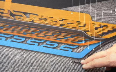
Warp knitting is an excellent candidate. It combines weaving and weft knitting, allowing the warp knitted fabrics to have the stability of woven fabrics and the elasticity of knitted ones.
Conformal EMI shielding is a megatrend on its way to become ubiquitous in electronics. The incumbent process is based on sputtering a tri-layer structure consisting of SUS on the EMC of the package. In these slides, you can see performance analysis and detailed cost analysis/projections.
This article describes the TAeTTOOz printable battery technology developed by Evonik and acquired by InnovationLab for upscaling and mass production. In this article, you can learn about the operating principles, the key working characteristics, the material set, production techniques, and emerging applications of this technology
An instrumentation amplifier is a precision differential amplifier designed to amplify small voltage differences. This guide explains the three-op-amp architecture, and how to choose between INA128, AD620, LT1167, and a standard difference amplifier for sensor front-ends.
A guide covering the full radio-frequency design workflow, starting from setting specifications and choosing topologies to matching, simulation, layout, and verification, to help antenna engineers.
This article presents a detailed technical exploration of SiC MOSFET devices, covering material physics, device structure, switching behavior, and practical design considerations for high-efficiency power electronics systems.
This article is a comprehensive technical guide to relay wiring diagrams, covering 4-pin and 5-pin configurations, working principles, safety practices, standards, and advanced relay applications in modern systems.
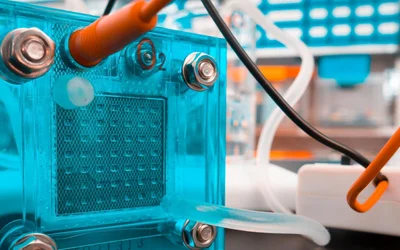
The integrated design achieves accurate micro gas chromatography and can help reduce the cost of monitoring chemical synthesis, natural gas pipelines or at-home air quality.
Hybrid bonding provides the adhesive free, copper to copper interconnects that are driving cutting edge 3D chip stacking. This article explains the theory, process, benefits, challenges, applications, and emerging trends of hybrid bonding for engineers.
Warp knitting is an excellent candidate. It combines weaving and weft knitting, allowing the warp knitted fabrics to have the stability of woven fabrics and the elasticity of knitted ones.
Conformal EMI shielding is a megatrend on its way to become ubiquitous in electronics. The incumbent process is based on sputtering a tri-layer structure consisting of SUS on the EMC of the package. In these slides, you can see performance analysis and detailed cost analysis/projections.
This article describes the TAeTTOOz printable battery technology developed by Evonik and acquired by InnovationLab for upscaling and mass production. In this article, you can learn about the operating principles, the key working characteristics, the material set, production techniques, and emerging applications of this technology
Why can microLED technology can help narrow the energy gap in electronic devices? The first slide shows the battery gap- Ahmed (Intel) has collected data by year showing that power demand of phones far exceeds the power supply level of batteries, creating a "battery gap" which ...
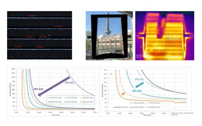
The progress of screen printing towards fine line printing has been incredible going from 100 µm features before 2010 to 70 µm to 2015 to 40 µm in 2018 and now pushing - in development- towards 20 µm and less. In parallel, the wet thickness of the printed line have gone down from 12um or so in 2018 to now just 4um.
As microLEDs inevitably shrink in size, the micro-bumping requirements for the microLED dies becomes more challenging. Direct wafer-based printing based on gravure offset techniques offers a promising solution in this regard. Indeed, this is another field where printed electronics can play a role.
The three themes are closely linked since QDs can be digitally printed as color conversation materials atop blue microLEDs to enable wide color gamut RGB uLED displays without requiring a separate transfer step for each color.. This is an important technology as it simplifies the manufacturing step for microLED and thus removing a major hinderence.
PCB layers are the copper layers within a printed circuit board, laminated between or onto layers of conductive material. These layers are stacked to enhance the functionality of electronic devices. This article explores the concept of PCB layering, the various types of layers, and their benefits.

In this article, we look at how Super Low power Wi-Fi and Bluetooth LE enable smart locks to be more agile and reliable by demonstrating these features with a case study from Renesas.
The EVT Stage implements the design in its form, fit, and function to better inform stakeholders of your production intent. Don't rush this important milestone.
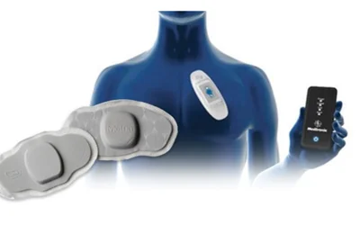
Flexible electronics have enabled the design of sensors, actuators, microfluidics and electronics on flexible, conformal and/or stretchable sublayers for wearable, implantable or ingestible applications.
Article #3 of the Enabling IoT Series. This article looks at how Time of Flight (ToF) sensors are used for this purpose and are changing the way we can interact with VR, and other video technologies.