Electronics


This guide is written for engineers and technical teams building connected devices who need clear, field-ready guidance without getting lost in standards documentation.
PCB Trace Width Calculator


In this article, we will discuss the different aspects of an effective ink delivery system. We will focus on a recirculating inkjet system as they are highly in demand in industry, especially where functional fluids come into play.

Gesture recognition, leveraging the advanced capabilities of embedded devices and streamlined through specialized platforms is creating new means of human-machine interactions, paving the way for more intuitive and user-friendly device interfaces.

Engineers Wiki. Most Asked Questions.
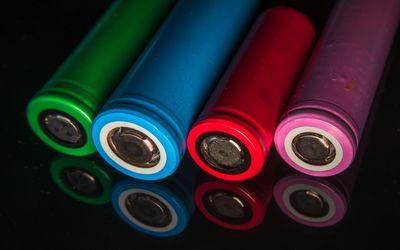
Understanding the key differences between the two high-in-demand battery types. This article focuses on Energy density, lifespan, safety, and cost trade-offs for the technical selection of Li-Ion and LiFePO4 batteries.
DC Motor Speed Control: PWM Techniques for Brushed and BLDC Drives
16 minutes read.
Crystal Oscillator: Fundamentals, Models, and Design Guidelines
20 minutes read.
What Is LiFePO4? Engineering Guide to Lithium Iron Phosphate Batteries
15 minutes read.
Bandgap Voltage Reference: Complete Guide for Analog Engineers
20 minutes read.
How to Charge a Lithium-Ion Battery Safely and Efficiently?
13 minutes read.
Voltage Reference: A Survey for Precision Engineers
28 minutes read.
ORGANIZATIONS. SHAPING THE INDUSTRY.

Mouser Electronics
Electronics
Mouser Electronics is a worldwide leading authorized distributor of semiconductors and electronic components.
219 Posts


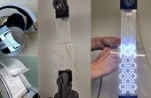
TAGGED WITH flexible electronics
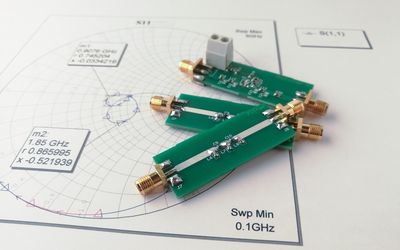
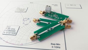
A guide covering the full radio-frequency design workflow, starting from setting specifications and choosing topologies to matching, simulation, layout, and verification, to help antenna engineers.
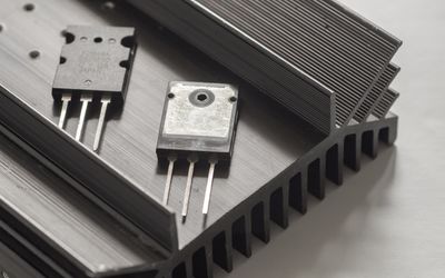
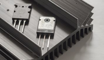
This article presents a detailed technical exploration of SiC MOSFET devices, covering material physics, device structure, switching behavior, and practical design considerations for high-efficiency power electronics systems.
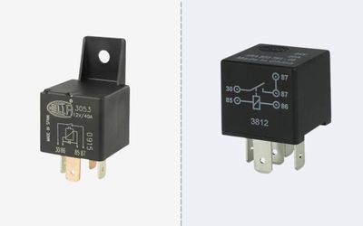
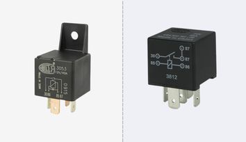
This article is a comprehensive technical guide to relay wiring diagrams, covering 4-pin and 5-pin configurations, working principles, safety practices, standards, and advanced relay applications in modern systems.
Explore how frequency shapes EMC behavior from RF emissions to ultra-low-frequency drift, with mitigation strategies for robust, compliant electronic system design.
TAGGED WITH microchips
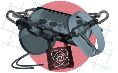
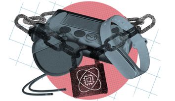
Ultra-efficient chip design enables extremely strong cryptography algorithms to run on energy-constrained edge devices.

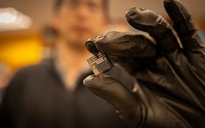
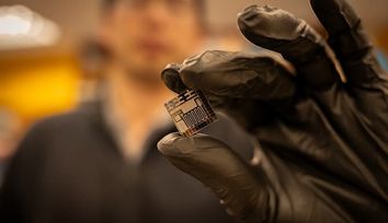
Researchers at ETH Zurich have now developed chip technology that enables verification of the authenticity of sensor data, including images or videos.

The integrated design achieves accurate micro gas chromatography and can help reduce the cost of monitoring chemical synthesis, natural gas pipelines or at-home air quality.

Hybrid bonding provides the adhesive free, copper to copper interconnects that are driving cutting edge 3D chip stacking. This article explains the theory, process, benefits, challenges, applications, and emerging trends of hybrid bonding for engineers.
Latest Posts
InDro Robotics expands with InDro Forge

5 minutes read
In this article, we will discuss the different aspects of an effective ink delivery system. We will focus on a recirculating inkjet system as they are highly in demand in industry, especially where functional fluids come into play.

8 minutes read
Gesture recognition, leveraging the advanced capabilities of embedded devices and streamlined through specialized platforms is creating new means of human-machine interactions, paving the way for more intuitive and user-friendly device interfaces.

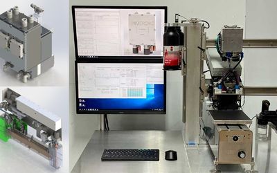
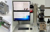
Catching and rectifying defects early can save businesses time, effort, and capital, giving companies a competitive advantage.

7 minutes read

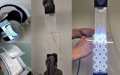
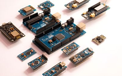
A growing desire for continuous data collection, real-time information, and connectivity has resulted in increased demand for electronic functionalities that are fully integrated in everyday objects. Consumer electronics, healthcare, wearable electronics, IoT, and smart packaging ...
9 minutes read
FR4, often called "fiberglass," quietly underpins our daily lives. Think about your electronics, from smartphones to car and appliance circuit boards. FR4 is the unsung hero behind the scenes, making them work smoothly and power our modern world.


How a hand-built electric race car from Swiss university students shattered the 0-62mph (0-100km/h) acceleration record in a mere 0.956 seconds, outpacing the giants of the automotive world.


Conversational AI enables machines to respond in a human-like manner. These intelligent systems are designed to understand intent and context, remember user preferences, and engage in meaningful conversations.

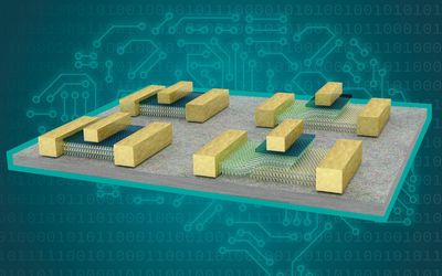
FPGAs are reconfigurable hardware used for parallel, high-speed processing, while microcontrollers are fixed-architecture chips designed for sequential, control-oriented tasks. FPGAs offer flexibility and performance MCUs provide low power, ease of use, and cost-efficiency.

Enclosures can become heat traps, so thermal management is crucial.
4 minutes read


Smart lighting company Signify reports that replacing conventional street lighting with energy-efficient LEDs is an effective way to reduce energy consumption and associated emissions.

5 minutes read

The fusion of 2D semiconductors and ferroelectric materials could lead to joint digital and analog information processing, with significant improvement in energy consumption, electronic device performance, and lead to novel functionalities.


In the dynamic landscape of retail stores, bars, clubs, and seasonal markets, the need for effective product visibility becomes even more evident. Illumination technologies are amongst the highly effective means for brand distinction and impactful visual communication.
7 minutes read


Identify gaps in current assistive technologies and design innovative solutions that cater to the unique needs of individuals with disabilities. Win great prizes.


Air Quality Indexes (AQIs) are used to measure the concentration of pollutants like particulate matter and other harmful substances in the air outside.