Demystifying Soldering Techniques: A Comparison of Wave Soldering and Reflow Soldering
Soldering Unveiled: Exploring Wave and Reflow Techniques for Engineering Graduates. Delve into the Depths of PCB Assembly, Component Compatibility, Production Efficiency, and Quality Assurance. Gain Profound Insights into Wave Soldering Machines, Reflow Ovens, and the Art of Soldering. Empower Your Engineering Journey with this In-Depth Comparative Analysis of Two Key Soldering Methods.

26 May, 2023. 14 minutes read
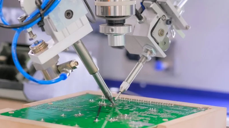
Process of selective soldering components to printed circuit boards at factory, exhibition - close up view. Automated technology, industrial, robotic, electronic, production, manufacturing concept
1. Introduction
Soldering, an essential process in electronics manufacturing, plays a crucial role in ensuring reliable and durable connection between components. Two widely used soldering techniques, namely wave soldering and reflow soldering, have revolutionized the industry with their efficiency and precision. Each method has its own unique advantages and disadvantages, which makes it essential for engineers, designers, and manufacturers to understand the differences between the two processes. In this article, you will delve into the world of soldering, demystifying wave soldering and reflow soldering, comparing the principles, processes, and applications in the context of printed circuit board (PCB assembly). You will also explore key terms such as wave soldering machines, solder joints, surface mount technology, and more. By the end of this article, you'll have a solid foundation of both soldering techniques, enabling you to make informed decisions and contribute effectively to the ever-evolving world of electronics engineering.
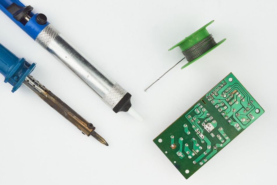
2. Wave Soldering
Wave soldering is a well-established soldering technique, commonly used in the electronics manufacturing industry. It is particularly suited for soldering through-hole components and offers several advantages in terms of speed, consistency, and reliability. In this section, you will explore the fundamentals of the wave soldering process, its advantages, and disadvantages, and how it compares to reflow soldering in various aspects.
2.1 The Wave Soldering Process
Wave soldering process involves the use of a specially designed machine that creates a "solder wave" by pumping molten solder through a nozzle. This solder wave is then utilized to solder the electronic components to the PCB. The process can be broken down into following main stages:
- Flux Application: Before Soldering, a flux is applied to the PCB. The flux, such as solder flux, serves multiple purposes. It cleans the surface of the PCB and component leads, removing oxidation that can hinder proper solder wetting. The flux also helps in the prevention of solder bridging and provides protection against thermal shock and oxidation during the wave soldering process.
- Preheating: Preheating is a crucial step in the wave soldering process. The PCB assembly is preheated to a specific temperature range, typically between 2-6°C, which helps to minimize thermal shock to electronic components, during the soldering process. Preheating also aids in the evaporation of solvents present in the flux, ensuring a more controlled and reliable soldering environment.
- Wave Generation: A wave soldering machine, equipped with a solder pot, generates the wave of molten solder. The solder pot contains a molten solder alloy, often lead-free solder, maintained at a specific temperature typically ranging from 1-3°C. The solder wave height and shape can be adjusted to suit the PCB design and component requirements, ensuring thorough wetting and coverage of the desired solder joints.
- PCB Assembly Passage: The PCB assembly, consisting of components such as through-hole and surface mount components, is carefully positioned over the wave of molten solder. The conveyor system moves the PCB assembly across the wave in a controlled manner, allowing the solder to flow and create strong connections. Through-hole components, with leads passing through the PCB, are particularly suitable for wave soldering, as the solder wave effectively contacts the leads, forming reliable solder joints.
- Cooling and Solidification: After passing through the wave, the PCB assembly enters a cooling zone. Proper cooling is essential to ensure the solidification of the solder joints, preventing components from shifting before the solder completely solidifies. This cooling process helps minimize the occurrence of thermal shock and potential defects, such as solder joint fractures or component damage due to rapid temperature changes.
2.2 Advantages of Wave Soldering
Wave soldering offers several benefits for electronics manufacturing, particularly when it comes to through-hole component assembly. Some of the main advantages of this soldering technique include:
- High Speed Soldering: One of the primary benefits of wave soldering is its speed. The process is highly efficient, as multiple components can be soldered simultaneously as the PCB passes over the solder wave. This allows for faster assembly times, making it an ideal solution for high-volume production runs. The conveyor speed, typically ranging from 1-3 cm/s, can be adjusted to accommodate different PCB sizes and production requirements.
- Through-hole component soldering: Wave soldering is particularly suitable for through-hole components, where the solder wave can effectively contact the leads and create robust solder joints. The thorough wetting and the formation of intermetallic compounds between the solder and the leads contribute to the mechanical strength and long-term reliability of the solder joints.
- Reliable Solder Joints: The wave soldering process ensures good wetting and reliable solder joints due to the thorough contact of the molten solder with the component leads and PCB pads. The controlled wave height, solder temperature, and conveyor speed contribute to the formation of uniform, void-free, and mechanically robust solder joints, essential for the long-term functionality and reliability of electronic assemblies.
- Cost Effective Solution: Wave soldering can be a cost-effective solution, particularly for large-scale manufacturing. It eliminates the need for individual soldering of through-hole components, reducing manual labor and associated costs. Additionally, the availability of lead-free solder alloys and efficient fluxes helps comply with environmental regulations while maintaining high-quality solder joints.
2.3 Disadvantages of Wave Soldering
Despite its numerous advantages, wave soldering does have some limitations and drawbacks. Some of the main disadvantages of this soldering technique include:
- Unsuitable for Surface Mount Technology Components: Wave soldering is not suitable for surface mount components (SMD), which have small, delicate leads or pads that can be easily damaged or dislodged by the high-temperature molten solder wave. For SMT components, reflow soldering is the preferred method, which allows precise control of soldering temperatures and avoids excessive thermal stress on the components.
- Limited Component Accessibility: The wave soldering process may limit access to specific areas of the PCB, making it difficult to solder components that require precision placement or delicate soldering techniques. In such cases, selective soldering or manual touch-up soldering methods may be necessary to ensure proper soldering in confined or hard-to-reach areas.
- Potential Solder Bridging the Bridging Effects: Solder bridging can occur when excess solder connects adjacent pads or leads, causing short circuits. The optimization of process parameters, such as wave height, solder temperature, and conveyor speed, is crucial to mitigate this issue. Proper design considerations, such as appropriate spacing and stencil design, also help minimize the risk of solder bridging.
- Thermal Stress Warpage: The high-temperature wave soldering process can subject the PCB assembly to thermal stress, potentially leading to warpage or damage to sensitive components. Proper preheating and cooling techniques, along with the selection of suitable materials, can help minimize these effects. Additionally, the use of pallets or fixtures during wave soldering can provide support and stability to the PCB assembly, reducing the risk of warpage and ensuring consistent soldering quality.
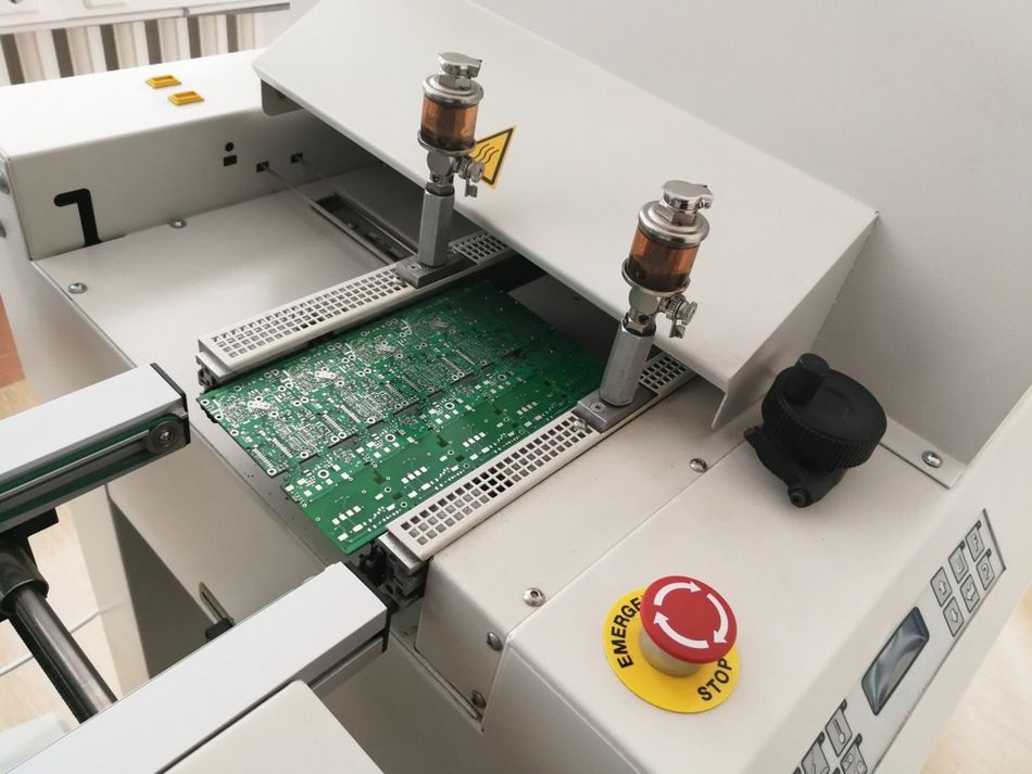
3. The Reflow Soldering Process
The reflow soldering process is a multi-step procedure that involves applying solder paste to a printed circuit board (PCB), placing surface-mount components on the paste, and then heating the assembly in a controlled environment to melt the solder and form reliable connections between the components and the PCB. The process can be broken down into several key stages:
- Solder Paste Application: Prior to soldering, solder paste, a mixture of solder alloy particles and flux, is applied to the PCB using a stencil. The solder paste is precisely deposited on the pads where the SMT components will be placed. The solder paste serves as a temporary adhesive and a source of solder for the reflow process.
- Component Placement: Surface Mount Technology components, with their delicate leads or pads, are carefully placed on the solder paste-covered pads of the PCB. Automated pick-and-place machines or manual assembly techniques are used for precise component placement. Proper component alignment and spacing are critical to ensure accurate soldering during the reflow process.
- Heating (Ramp-up): The PCB assembly, with the solder paste and components in place, undergoes heating in a reflow oven. The temperature gradually increased, typically between 2-4°C per second, to reach the reflow temperature. During this ramp-up phase, the flux in the solder paste activates, removing oxidation from the solder pads and component leads.
- Reflow: Once the desired reflow temperature is reached, typically between 2-4°C, the solder paste transforms from a solid to a liquid state, creating a metallurgical bond between the component leads and the PCB pads. The molten solder alloy flows, forming reliable solder joints as the surface tension pulls the liquid solder into the proper shape and position.
- Cooling and Inspection: After the solder has reflowed, the PCB assembly is allowed to cool down, solidifying the solder joints. The temperature is gradually reduced, typically at a rate of 1-2°C per second, allowing the solder joints to solidify and the assembly to reach ambient temperature. Proper cooling prevents thermal stress, warpage, and component damage.
3.1. Advantages of Reflow Soldering
Reflow soldering offers several benefits that make it an ideal choice for soldering surface Mount components in the electronics industry. Some of the primary advantages of reflow soldering include high:
- Enhanced Miniaturization and Packaging Density: Reflow soldering enables the assembly of compact and densely populated PCBs. The ability to accurately place and solder small Surface Mount Technology components allows for miniaturization and improved packaging density, leading to smaller and more efficient electronic devices. This advantage is especially crucial in industries such as consumer electronics, aerospace, and medical devices, where size and weight reduction are paramount.
- Suitability for Surface Mount Technology Components: Reflow soldering is particularly well-suited for soldering small surface-mount components with fine-pitch leads. Since the solder paste is applied to the PCB pads and the components are placed directly onto the paste, there is a reduced risk of solder bridges or insufficient solder joints that can occur with wave soldering. This makes reflow soldering an ideal choice for manufacturing high-density electronic devices.
- Reduced Risk of Defects: The controlled heating process in reflow soldering helps to minimize the risk of soldering defects. By gradually increasing the temperature and carefully controlling the temperature profile, reflow soldering ensures that the solder paste melts and solidifies correctly, forming reliable connections between the components and the PCB. This reduces the likelihood of defects such as solder bridges, cold solder joints, or solder balls.
- Energy Efficiency: Reflow soldering is generally more energy-efficient compared to wave soldering. Since the solder paste is applied only to the required areas of the PCB, there is less waste of solder material, which in turn reduces the overall energy consumption. Furthermore, the reflow process typically requires less heat energy than wave soldering, as the entire PCB assembly does not need to be immersed in molten solder. This contributes to lower overall energy consumption and reduced operational costs for manufacturers.
- No Solder Bridging: Unlike wave soldering, reflow soldering minimizes the risk of solder bridging between adjacent leads or pads. The precise deposition of solder paste, and the controlled heating process ensure that the solder stays confined to the designated areas, reducing the likelihood of short circuits. This advantage is crucial for complex PCBs with closely spaced components and high pin counts.
- Wide Range of Solder Alloys: Reflow soldering supports various solder alloys, including lead-free options, allowing compliance with environmental regulations while maintaining high-quality solder joints. Different solder alloys can be selected based on the specific application requirements, such as temperature resistance, reliability, or electrical conductivity. The ability to accommodate a wide range of solder alloys provides flexibility in product design and manufacturing.
3.2. Disadvantages of Reflow Soldering
Despite its numerous advantages, reflow soldering does have some drawbacks that should be considered when selecting a soldering method. Some of the main disadvantages of reflow soldering include:
- Sensitivity to Component and PCB Design: Reflow soldering is highly sensitive to component and PCB design considerations. Factors such as component size, thermal pad design, component warpage, and PCB layout can significantly impact the soldering process and the overall quality of solder joints. Inadequate thermal relief, improper pad design, or component misalignment can lead to issues like tombstoning, poor wetting, or insufficient solder joint formation.
- High Initial Equipment Cost: Setting up a reflow soldering process requires specialized equipment such as reflow ovens, temperature profiling tools, and solder paste inspection systems. The initial investment cost for such equipment can be relatively high, especially for small-scale or startup manufacturing operations. Additionally, the maintenance and calibration of the equipment also incur ongoing expenses.
- Potential for Component and PCB Damage: The high temperatures involved in reflow soldering can pose risks to sensitive electronic components and PCBs. Components with lower thermal tolerance, such as plastic-encapsulated devices, can experience heat-induced damage or deformation during the reflow process. PCBs with poor thermal conductivity or inadequate heat dissipation mechanisms may suffer from warpage or delamination.
- Process Complexity and Quality Control: Reflow soldering is a complex process that requires careful control of various parameters, including temperature profiles, solder paste deposition, and reflow atmosphere. Achieving consistent and reliable soldering results necessitates strict adherence to process control and quality assurance measures. Any deviations or variations in process parameters can lead to defects, such as voids, solder ball formation, or incomplete wetting.
Suggested reading: Solder Reflow: An In-Depth Guide to the Process and Techniques
4. Comparing Wave Soldering and Reflow Soldering
In this section, we will directly compare wave soldering and reflow soldering, taking into consideration their respective advantages and disadvantages. We will examine factors such as component compatibility, production volume, process control, and quality assurance to help manufacturers make informed decisions when choosing the most appropriate soldering method for their specific needs.
4.1 Component Compatibility
When it comes to component compatibility, wave and reflow soldering each have their unique advantages and limitations. Understanding the differences between the two methods is crucial for selecting the most suitable soldering process for a particular project.
- Wave Soldering Component Compatibility: Wave soldering is known for its versatility and compatibility with a wide range of components. It typically leads with a diameter ranging from 0.3mm to 3mm. The wave soldering process requires a solder temperature of approximately 250-270°C, ensuring proper wetting and solder joint formation. Through-hole components, such as connectors and switches, are commonly used in applications that require high mechanical strength and reliability, such as industrial automation and automotive electronics.
- Reflow Soldering Component Compatibility: Reflow soldering, on the other hand, is primarily suited for surface-mount components. The solder paste used in reflow soldering typically consists of a eutectic solder alloy, such as Sn63-Pb37 or lead-free alternatives like SAC305 (Sn96.5-Ag3.0-Cu0.5). The reflow process involves heating the PCB to a peak temperature of around 220°C to 250°C for a specific duration, typically ranging from 30 seconds to 90 seconds, depending on the component density and size. This ensures complete solder paste reflow, forming reliable solder joints between the SMT components and the PCB.
The choice between wave soldering and reflow soldering depends on the specific assembly requirements and the type of components used in the PCB design. Hybrid assembly processes may be employed to combine both wave soldering and reflow soldering techniques, accommodating different component types.
4.2 Production Efficiency
Efficiency is a crucial factor when evaluating soldering processes for manufacturing printed circuit boards. In this section, you will discuss the production efficiency of wave and reflow soldering, considering factors such as production volume, throughput, and overall process time.
- Wave Soldering Production Efficiency: Wave soldering is a batch process that allows simultaneous soldering of multiple PCBs. The conveyor speed in wave soldering machines typically ranges from 0.5 m/min to 2.5 m/min, enabling high-volume production. The setup and optimization of wave soldering parameters, such as wave height, preheating temperature, and dwell time, are crucial for achieving consistent soldering quality. Automated flux application systems ensure uniform distribution of flux on the PCBs, enhancing production efficiency.
- Reflow Soldering Production Efficiency: Reflow soldering is a sequential process where individual PCBs are soldered one at a time. The efficiency of reflow soldering can be improved by utilizing inline or continuous flow reflow ovens, which offer higher throughput rates compared to batch ovens. The conveyor speed in inline reflow ovens typically ranges from 0.5 m/min to 1.5 m/min, ensuring optimal heating and cooling profiles. Advanced reflow ovens equipped with multiple heating zones and precise temperature control contribute to enhanced production efficiency.
The production efficiency of wave soldering and reflow soldering depends on factors such as batch size, product complexity, and time constraints. Manufacturers need to consider their production requirements and cost-effectiveness when selecting the appropriate soldering technique.
4.3 Equipment and Setup Costs
When comparing wave and reflow soldering, it's essential to consider the costs associated with equipment and setup. These costs can have a significant impact on the overall budget for a manufacturing project. In this section, you will discuss the equipment and setup costs associated with wave soldering and reflow soldering, as well as the factors that can influence these costs.
- Wave Soldering Equipment and Setup Costs: Wave soldering requires specialized equipment, including a wave soldering machine and a solder pot. The cost of a wave soldering machine can range from $20,000 to $100,000, depending on the production capacity, features, and automation capabilities. Additionally, proper setup and calibration of the machine, including wave height adjustment, fluxing system alignment, and conveyor speed control, are critical for achieving consistent soldering results.
- Reflow Soldering Equipment and Setup Costs: Reflow soldering equipment includes a reflow oven, stencil printer, and solder paste inspection systems. The cost of a reflow oven typically ranges from $50,000 to $300,000, depending on the size, heating zones, and advanced features like nitrogen atmosphere capability. Additional costs are associated with stencil printers for precise solder paste deposition and solder paste inspection systems for quality control. The overall setup cost also includes the selection of appropriate solder pastes, which can vary in price depending on the composition and brand.
The choice between wave soldering and reflow soldering involves considering the initial investment, maintenance expenses, and the scale of production. Manufacturers need to evaluate their budgetary constraints and long-term operational requirements when deciding on the appropriate soldering technique.
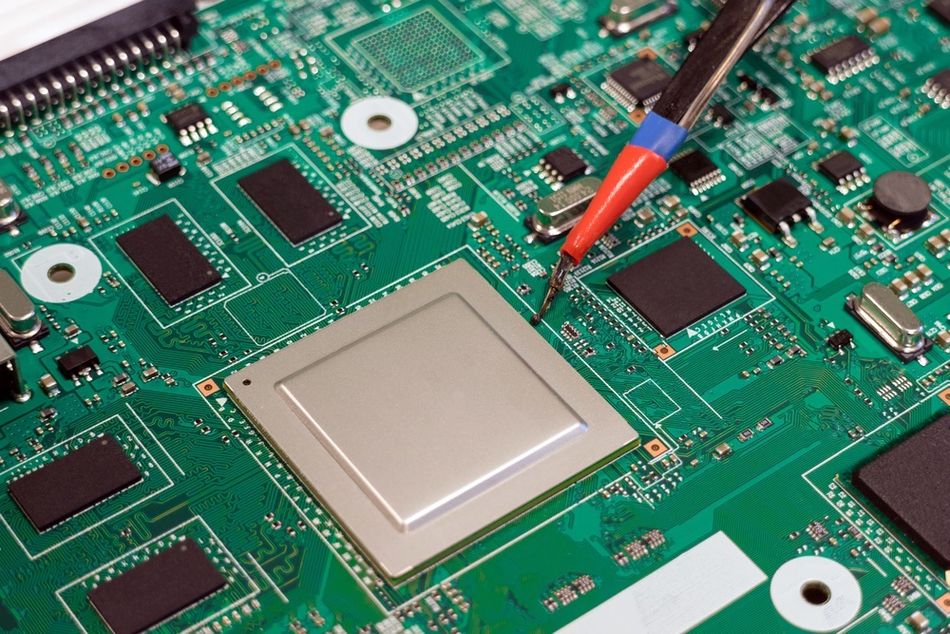
4.4 Quality and Reliability
When comparing wave and reflow soldering, it is important to consider the quality and reliability of the resulting solder joints, as these factors can significantly impact the performance and lifespan of electronic products. In this section, we will discuss the factors that influence the quality and reliability of solder joints in both wave and reflow soldering processes.
- Wave Soldering Quality and Reliability: Wave soldering provides robust mechanical connections and reliable solder joints. However, challenges such as bridging, solder ball formation, or insufficient wetting may arise if process parameters are not carefully controlled. Advanced wave soldering machines equipped with nitrogen inerting capability help minimize oxidation and improve solder joint quality. Proper flux selection and application techniques, as well as optimized preheating temperatures and conveyor speed, contribute to high-quality soldering results and improved reliability.
- Reflow Soldering Quality and Reliability: Reflow soldering offers precise control over the soldering process, leading to consistent and reliable solder joints. The optimization of temperature profiles, including ramp-up, soak, and cooling rates, is crucial for preventing thermal stress and minimizing defects like solder voids or tombstoning. Advanced reflow ovens with accurate temperature control, thermal profiling capabilities, and support for nitrogen or controlled atmosphere soldering contribute to enhanced solder joint quality and overall reliability.
To ensure high-quality solder joints, manufacturers should adopt comprehensive quality control measures, including solder paste inspection, inline inspection systems, and process optimization techniques. This helps minimize defects, enhance reliability, and meet the industry's quality standards.
5. Conclusion
The comparison of wave soldering and reflow soldering techniques provides valuable insights for engineering students and professionals in the field of electronics manufacturing. Wave reflow soldering excels in soldering through-hole components, offering robust mechanical connections and high current carrying capacity. While reflow soldering is ideal for surface mount technology components, providing precise control and consistent soldering results. Each technique has its own advantages and considerations in terms of component compatibility, production efficiency, equipment cost, and solder joint quality. By understanding the strengths and limitations of these methods, engineers can make informed decisions to optimize the soldering process and ensure high-quality PCB assemblies.
6. References
- The Use of Bismuth Alloy Systems for Reflow and Wave Soldering | Emerald Insight
- Wave Soldering of SMDs—A Smart Approach From Science to Practice | Emerald Insight
- Lead‐free reflow soldering for electronics assembly | Emerald Insight
- A Comparison of Reflow Soldering and Wave Soldering - Industry Articles (allaboutcircuits.com)
- Reflow Soldering and Wave Soldering: Difference and Process (nextpcb.com)
Frequently Asked Questions (FAQs)
- What is the main difference between wave soldering and reflow soldering?
The main difference lies in the soldering process. Wave soldering uses a molten solder wave to create solder joints, while reflow soldering uses solder paste and a controlled thermal profile to form solder joints. Wave soldering is more suited for through-hole components, while reflow soldering is typically used for surface-mount components. Wave soldering is typically used for through-hole components, while reflow soldering is suitable for surface mount technology components.
- Can both wave and reflow soldering be used for surface-mount components?
Reflow soldering is the preferred method for surface -mount components, wave soldering can also be used for some surface mount technology components, it may not be suitable for densely populated or fine-pitch components.
- How important is the soldering temperature in both processes?
Soldering temperature is crucial in both wave and reflow soldering. In wave soldering, the solder wave temperature usually ranges between 250°C and 270°C, while in reflow soldering, the peak temperature is typically between 235°C and 250°C. Proper temperature control is essential for achieving high quality solder joints, minimizing defects, and ensuring the overall integrity of the electronic assemblies.
- Is one soldering method more cost-effective than the other?
The cost-effectiveness of each method depends on the specific requirements of a project. Wave soldering can be more cost-effective for large-scale production, while reflow soldering can offer flexibility for smaller volumes and complex designs.
- What are some common soldering defects that can occur in wave and reflow soldering processes?
Common soldering defects in wave soldering include solder bridging, cold solder joints, and incomplete wetting. In reflow soldering, typical defects include tombstoning, voiding, and insufficient soldering. Proper process control and optimization can help minimize these defects and ensure the quality and reliability of solder joints in both methods.