How are Semiconductors Made? A Comprehensive Guide to Semiconductor Manufacturing
Silicon, with its abundant availability and unique properties, serves as the fundamental building block for semiconductor manufacturing. Its semi-metallic nature makes it an ideal material for controlled conduction of electricity. Furthermore, the combination of silicon with oxygen produces silicon dioxide, a crucial insulating component in silicon chip manufacturing.

02 Jun, 2023. 16 minutes read
1. Introduction
In today's digital age, semiconductors play an invaluable role in our everyday lives. They form the heart of all electronic devices we depend on — from smartphones and computers to cars and washing machines. In its essence, the process of creating semiconductors involves intricate scientific techniques and precise engineering. This guide is designed to delve into the complex world of semiconductor manufacturing, shedding light on how these tiny, yet powerful components are made.
Semiconductors are the unsung heroes that power the electronic devices we rely on daily. From the smallest microchips to the most advanced processors, semiconductors form the backbone of technology, enabling the seamless functioning of smartphones, computers, cars, and much more. Behind the scenes, a complex and precise manufacturing process brings these tiny but mighty components to life. This comprehensive guide aims to demystify the world of semiconductor manufacturing, providing an in-depth exploration of how these remarkable creations are made, from the raw materials to the final product.
2. The Raw Material: Silicon
Silicon, the second most abundant element on Earth, is the foundation for semiconductors. Comprising about 28% of the Earth's crust by mass, Silicon's semi-metallic nature makes it a prime choice in semiconductor production. It's not just the availability of silicon that makes it attractive, but also its specific physical and chemical properties. Silicon has four valence electrons that form covalent bonds leading to a stable crystal lattice structure. This property renders it as an ideal semiconductor material, allowing controlled conduction of electricity.
Furthermore, silicon is a resilient material that can withstand high temperatures, a necessary attribute given the extreme thermal processes involved in semiconductor manufacturing. Additionally, silicon dioxide, the result of combining silicon with oxygen, is an excellent insulator and is used in the manufacturing of silicon chips for this reason.
2.1. Silicon Mining
Silicon is predominantly sourced from silica (silicon dioxide), which is commonly found in sand and quartz. The process of silicon mining, in fact, involves the extraction of sand. Countries such as the United States, China, and Australia are top producers of silicon because of their abundant sand resources.
The process of silicon mining is somewhat similar to traditional mining. Sand, also known as Silicon dioxide (SO2), is first extracted from the Earth through open pit mining or dredging. After extraction, the sand undergoes extensive cleaning and filtering processes to remove unwanted materials. The refined sand is then heated in a high-temperature furnace in the presence of carbon. This process, known as carbothermic reduction, results in the production of metallurgical grade silicon, with a purity level of about 98%.
This extracted silicon still contains impurities such as iron, aluminium, and other metals. Although this grade of silicon is used in other industries, such as metallurgy and chemical production, the production of semiconductors requires an even higher degree of purity. As such, further refinement processes are necessary to create semiconductor-grade silicon.
2.2. Purification of Silicon
After mining and initial refinement, silicon undergoes a series of purification steps to reach the ultra-pure grade suitable for semiconductor manufacturing. This semiconductor-grade silicon, also known as electronic-grade silicon (EGS), must be 99.9999999% pure - a requirement necessitated by the precise nature of semiconductor devices. Even trace amounts of impurities could drastically impact their functionality.
The purification process typically begins with the conversion of metallurgical grade silicon to a more volatile compound that can be further purified. This is accomplished through the Siemens process, where the metallurgical grade silicon is reacted with hydrochloric acid to produce trichlorosilane (HCl3Si). Trichlorosilane is a volatile compound that can be easily purified through distillation techniques.
This purified trichlorosilane is then subjected to a process called chemical vapor deposition (CVD) in a Siemens reactor. The CVD process involves passing hydrogen gas over the heated trichlorosilane, which decomposes the compound to produce highly pure silicon and hydrogen chloride. The resulting silicon is in a polycrystalline form and possesses the high purity level required for semiconductor manufacturing.
In recent years, an alternative method, known as the Fluidized Bed Reactor (FBR), has been increasingly used. It employs a similar principle as the Siemens process but does so more efficiently, thus reducing the cost of production. However, both methods aim for the same goal: to produce ultra-pure silicon suitable for semiconductor manufacturing. These purification processes illustrate the lengths to which manufacturers must go to ensure the necessary purity level, underlining the precision required in semiconductor production.
Recommended Reading: Magnetron Sputtering: A Versatile Thin Film Deposition Technique
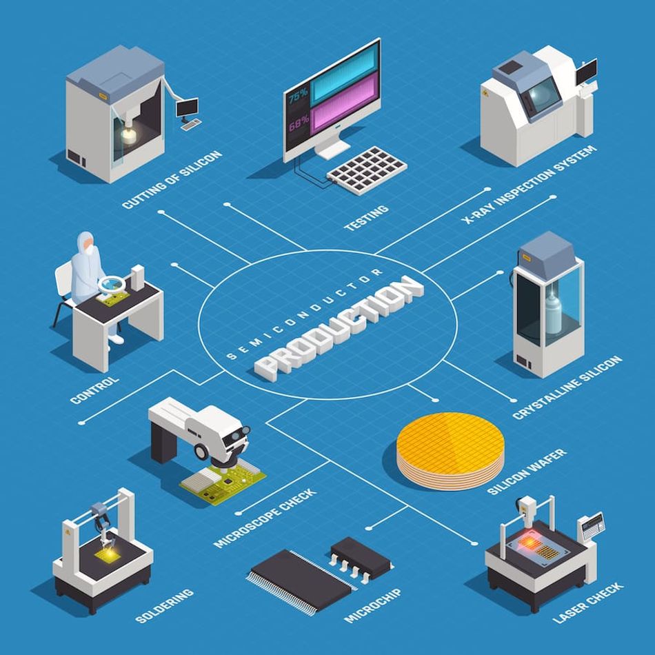 Semiconductor chip production isometric flowchart with isolated images of hi-tech factory facilities
3. Silicon Ingot Production
Once ultra-pure silicon is procured, it's time to shape it into a form suitable for chip production. The process begins by creating a silicon ingot, a large, cylindrical piece of silicon. Ingot production starts with a small piece of silicon, called a seed crystal, which is dipped into molten silicon and then slowly pulled upward while rotating. This technique, known as the Czochralski process, is essential for forming a cylindrical silicon ingot.
The silicon ingot, by the end of this process, is a single, continuous silicon crystal, often called a monocrystalline silicon. The monocrystalline nature of the ingot is crucial since it ensures uniformity of the crystal lattice structure, which is critical for reliable semiconductor functionality.
To manage the electrical characteristics of the final semiconductor devices, the silicon in the ingot is typically 'doped' during this stage. Doping involves introducing minute amounts of other elements, such as boron or phosphorus, into the silicon. These elements alter the silicon's electrical properties by adding additional free electrons or creating 'holes' where electrons can move.
3.1. Ingot Shaping and Sizing
Following the formation of the silicon ingot, it must be shaped and sized to meet the specifications necessary for chip manufacturing. The standard shape of these ingots is cylindrical, but they must be cut into thin, flat wafers to be usable in semiconductor devices. This transformation involves several precise machining processes.
The first step is to grind the cylindrical ingot into a uniform shape and size. This process is done to ensure that the ingot has a perfect cylindrical shape, with no bulges or imperfections. Next, the outer layer of the ingot is typically ground away to remove any potential contaminants that may have adhered during the previous processes.
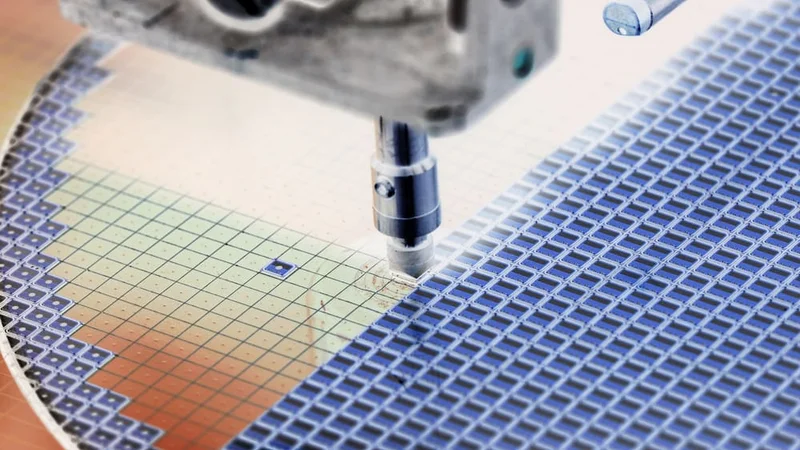
After the ingot is ground to a perfect cylinder, it is then cut into thin, flat discs known as wafers. These wafers are cut using a specialized saw that can maintain a high degree of precision. As technology advances and transistor sizes shrink, the requirement for thinness becomes more stringent. As of now, typical wafer thicknesses range from 675 to 725 micrometers.
The silicon wafers are then polished to a mirror finish, ensuring any remaining microscopic irregularities are removed. This high degree of surface smoothness is necessary to ensure accurate alignment and patterning in the subsequent steps of semiconductor production. It is the wafers from this process that will continue down the production line and eventually become the semiconductors in electronic devices.
4. Wafer Fabrication
Fabricating a wafer involves many intricate processes to transform a simple silicon disc into a platform for numerous microscopic electronic components. These processes include oxidation, lithography, etching, doping, and metallization.
Oxidation is the first step, where the silicon wafer is heated in an oxygen-rich environment. The result is a layer of silicon dioxide, which insulates the underlying silicon. Silicon dioxide can also serve as a 'mask' during later etching stages or as a 'gate' in transistors.
Next, lithography is employed to imprint the intricate circuit patterns onto the silicon dioxide layer. The process involves the application of a light-sensitive material called a photoresist onto the silicon dioxide. The photoresist is then exposed to ultraviolet light through a mask with the circuit pattern. This exposure causes the photoresist to harden in the pattern of the mask.
Following lithography, the wafer undergoes an etching process. The unhardened photoresist is removed, and an etching solution is applied to the wafer, removing the exposed silicon dioxide and leaving behind the desired pattern.
The wafer then undergoes doping to modify its electrical properties. This process involves introducing impurities into specific areas of the silicon wafer via diffusion or ion implantation. This step creates regions with distinct electrical properties, enabling the creation of p-n junctions – the building blocks of semiconductor devices.
Finally, metallization is carried out to provide a means of electrical connection between the different elements of the integrated circuit. Thin layers of metal, usually aluminum or copper, are deposited onto the wafer, connecting different parts of the circuit. After metallization, the wafer is typically coated with a protective layer to guard against damage and contamination.
Recommended Reading: Semiconductor Fabrication Process: The Ultimate Guide to Creating Cutting-Edge Electronics
4.1. Wafer Polishing
An essential process in wafer fabrication is wafer polishing, also known as chemical-mechanical planarization (CMP). Following the sequence of fabrication processes, the water'swafer's surface is left with various topographictopographical irregularities. These irregularities can hinder the lithographic process, where the depth of focus is critical.
Wafer polishing employs a combination of chemical and mechanical processes to reduce these topographical variations, yielding a flat, smooth surface. The wafer is placed on a rotating platen with a pad and a chemically active slurry. As the wafer is pressed against the pad and the platen rotates, the slurry aids in removing the material from the high points on the wafer, levellingleveling out the surface.
This process is critical to ensure the correct functioning of the semiconductor devices on the wafer. High precision is necessary, as the irregularities being removed are often just a few nanometers high. After CMP, the wafer is thoroughly cleaned to remove any residual slurry or debris before proceeding to the next fabrication step.
5. Layering Process
In the creation of semiconductor devices, the process of layering is an essential stage. Layering involves depositing different materials onto the silicon wafer, each with specific properties and functions. These materials can be classified into three primary categories: insulators, semiconductors, and conductors.
Insulator layers, often silicon dioxide, are deposited to electrically isolate different parts of the circuit. The insulator layer also protects the underlying layers from environmental contamination. The process of forming an insulator layer is known as thermal oxidation, where the silicon wafer is heated in the presence of oxygen to form a thin layer of silicon dioxide.
The semiconductor layers form the active regions of the device where the electrical activity takes place. These layers are typically composed of either pure silicon or a combination of silicon and other elements such as germanium. These layers are created through a process known as epitaxy, where layers of semiconductor material are grown on the silicon wafer.
Finally, conductor layers are deposited to create connections between different parts of the circuit. These connections allow the flow of electricity through the device. Metals like aluminum or copper are typically used for conductor layers.
5.1. Oxidation
Oxidation is a fundamental process in the formation of the insulator layers during the layering process. It involves the controlled heating of the silicon wafer in an oxygen-rich environment, causing a thin layer of silicon dioxide (SiO2) to form on the wafer's surface. Silicon dioxide acts as an excellent insulator due to its high breakdown voltage, around 10^6 volts per centimeter, and low leakage current.
Two common types of oxidation processes are wet oxidation and dry oxidation. Wet oxidation, where steam is passed over the wafer at high temperatures (typically above 1000 degrees Celsius), results in a thicker oxide layer and is faster than dry oxidation. Dry oxidation, on the other hand, uses dry oxygen at similar temperatures, producing a thinner, denser, and higher quality oxide layer.
The thickness of the oxide layer is critical and highly controlled as it directly influences the device's electrical properties. For instance, in a metal-oxide-semiconductor field-effect transistor (MOSFET), the gate oxide thickness can significantly affect the transistor's threshold voltage. Modern processes can control the oxide thickness down to a few nanometers.
6. Dopant Diffusion
Dopant diffusion is an essential step in semiconductor fabrication, giving semiconductors their characteristic property of charge control. The process involves incorporating impurity atoms, known as dopants, into the silicon wafer. Depending on the type of dopant used, the silicon can be made either n-type (majority carriers are electrons) or p-type (majority carriers are holes).
For instance, phosphorus or arsenic, having five valence electrons, can be used to create n-type silicon. In contrast, boron or gallium, having three valence electrons, is used to create p-type silicon. These impurities replace silicon atoms in the crystal lattice, contributing extra charge carriers. The concentration of these dopants can be as low as one dopant atom per million silicon atoms, but it significantly influences the electrical properties of the silicon.
Dopant diffusion is carried out at high temperatures, typically in the range of 900 to 1200 degrees Celsius. The silicon wafer is placed in a furnace, and the dopant source is introduced as a gas. The dopants diffuse into the silicon wafer, driven by the temperature gradient, and take up positions within the silicon's crystal lattice.
The process is highly controlled, as the depth of the diffusion, known as the junction depth, directly impacts the device's electrical characteristics. It typically ranges from a few hundred nanometers to several micrometers, and it is measured using techniques such as secondary ion mass spectrometry (SIMS). The resulting junction's abruptness can affect the performance of semiconductor devices. An abrupt junction is critical in devices like bipolar junction transistors (BJTs), whereas a more gradual junction is required for devices like MOSFETs.
7. Etching Process
The etching process is an essential step in semiconductor fabrication used to remove selected layers from the surface of a silicon wafer. It allows the creation of intricate patterns that form the basis for the miniaturized circuits present in the electronic devices. The etching process can selectively remove silicon dioxide, polysilicon, metal layers, or even the silicon substrate itself. The patterns are defined using photolithography, where a photosensitive material called a photoresist is exposed to light, defining regions to be protected during etching.
Etching can be performed using two methods: wet etching and dry etching. Wet etching uses a liquid etchant to dissolve away the material. This method is cost-effective and straightforward. However, it has limitations such as isotropic etching, meaning it etches equally in all directions, which can lead to undercutting the patterns. The isotropic nature of wet etching makes it difficult to achieve high aspect ratios (depth to width ratio) in the etched features.
Dry etching, on the other hand, employs gas phase etchants in a vacuum chamber, and offers higher control over the etch process. A prevalent dry etching technique is reactive-ion etching (RIE). In RIE, a plasma of reactive ions is generated using a radio frequency (RF) source. These ions are accelerated towards the wafer where they react with the surface material, converting it into a volatile byproduct that can be removed by vacuum pumping. The directionality of ion bombardment in RIE results in anisotropic etching, allowing the creation of high aspect ratio features with vertical sidewalls.
The etching process must be carefully controlled, and one key parameter is the etch rate, typically measured in nanometers per minute. Factors such as temperature, pressure, and the composition of the etching agent can all affect the etch rate. In the case of dry etching, additional factors such as RF power and chamber pressure play crucial roles. Variations in the etch rate across the wafer, known as etch uniformity, is another vital parameter that is carefully controlled to ensure uniform feature sizes across the wafer.
These precision-controlled etching processes enable the production of nanoscale structures, with feature sizes now reaching below 10 nanometers in leading-edge semiconductor devices. This capability is fundamental to the continuing miniaturization of electronic circuits, which drives improvements in performance, energy efficiency, and cost.
Recommended Reading: Understanding Plasma Etching: Detailed Insights into Its Techniques, Uses, and Equipment Maintenance
 Automated soldering machine inside at industry
8. Final Steps: Testing and Packaging
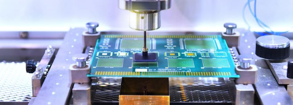
In the last stages of semiconductor fabrication, the focus shifts from manufacturing to assurance of quality and protection. The testing stage is integral to the manufacturing process and is performed to ensure that all the circuits on the wafer function correctly. A suite of electrical tests are performed, referred to as wafer probing or wafer testing. This involves contacting each of the die on the wafer with an array of tiny probes that are connected to a tester. The tester runs a series of electrical tests, checking parameters like current, voltage, resistance, and capacitive or inductive properties. These tests are designed to ensure that the device meets all its specification and functionality requirements. An automatic test pattern generation (ATPG) software is commonly used to generate the test vectors (input combinations).
Following testing, nonfunctional dies are marked, and the wafer is sliced into individual chips in a process known as dicing. Dicing is typically performed using a precision diamond saw that cuts along the streets between dies. Each die or chip is then mounted into a protective package which provides a robust environment for the die and facilitates connections to the outside world. Packaging methods vary widely based on application requirements and the trade-off between cost and performance. In the simplest form, the chip can be encapsulated in plastic with thin wires connecting the chip to the external leads. More advanced techniques involve flipping the chip upside down (flip-chip packaging) and soldering it directly to the package leads for better electrical performance.
Post-packaging, the chips undergo final testing to ensure they survived the packaging process intact and are still functional. They are also tested under different environmental conditions like temperature and humidity to ensure reliability. If the chip is part of a larger system on a chip (SoC), it might go through functional testing where all the subsystems are checked for correct operation. In these advanced stages, defects are typically extremely low, but any found at this stage result in the discarding of the entire chip. This underscores the importance of early and consistent quality control in earlier stages of the fabrication process.
In terms of numerical data, testing can be a time-consuming process. It is not uncommon for testing to account for up to 25% of the total manufacturing time. The test coverage – the percentage of a chip's functionality that is tested – can exceed 99% for high-reliability applications like automotive or aerospace. The average chip yield – the percentage of functional chips on a wafer – varies widely based on the complexity of the process and the maturity of the technology, but it can range from 50% for new, leading-edge processes to over 90% for mature, well-understood processes.
9. Challenges in Semiconductor Manufacturing
Semiconductor manufacturing is a complex, multidisciplinary process that faces a number of challenges. These challenges encompass technical, economic, and environmental aspects.
Continous Push for Miniaturization:
One significant technical challenge in semiconductor manufacturing is the continuous push for miniaturization. The demand for higher transistor density and lower power consumption drives the need for ever-smaller transistor dimensions. This has led to the development of processes that can create features that are only a few nanometers in size, far smaller than the wavelength of visible light. This extreme miniaturization presents numerous technical challenges, such as controlling feature size and placement with high precision, and managing the increasing influence of quantum mechanical effects on device behavior.
Yield Management:
Yield management is another challenge that is associated with miniaturization. Associated with miniaturization is the challenge of yield management. As chips become more complex and feature sizes shrink, the potential for defects that can render a chip nonfunctional increases. Consequently, managing yield – the percentage of good chips on a wafer – becomes a major challenge. Techniques such as fault tolerance and redundancy are employed to mitigate the impact of defects, but these add complexity and cost to the chip design process.
Economical Challenges:
Economic challenges in semiconductor manufacturing are largely driven by the high costs associated with new technology development and fab construction. For example, a modern fab capable of manufacturing chips with sub-10 nanometer features can cost upwards of $10 billion to construct. This high cost of entry means that only a handful of companies worldwide can afford to remain at the cutting edge of technology, which impacts competition and innovation in the sector.
Environmental Challenges:
Environmental challenges in semiconductor manufacturing relate to the significant resources required for the process. Manufacturing a single 300mm silicon wafer can require thousands of liters of ultra-pure water, large amounts of electricity, and a variety of chemicals, some of which are hazardous. Therefore, effective resource management and waste disposal are significant challenges for the industry.
The Need for Continuous Innovation:
Lastly, semiconductor manufacturing is also challenged by the need for continuous innovation. As existing semiconductor technologies approach their fundamental limits, new technologies need to be developed. Examples include new transistor designs such as FinFETs and nanowire transistors, new materials like graphene and carbon nanotubes, and entirely new computing paradigms such as quantum computing. These innovations present challenges in terms of the fundamental science and engineering required to make them viable, as well as the need for significant investment in new manufacturing processes and equipment.
10. Future Trends in Semiconductor Manufacturing:
The semiconductor industry is continuously evolving, driven by the demand for faster, smaller, and more power-efficient devices. Several emerging trends are shaping the future of semiconductor manufacturing. Here are some key areas to watch:
Advanced Process Nodes:
Moore's Law, which states that the number of transistors on a chip doubles approximately every two years, has driven semiconductor miniaturization for decades. This trend is expected to continue with the development of advanced process nodes, such as 5 nanometers (nm) and beyond. These smaller nodes enable higher transistor density, improved performance, and reduced power consumption.
Three-Dimensional (3D) Integration:
3D integration involves stacking multiple layers of chips vertically, enabling increased functionality and performance in a smaller form factor. Through-silicon vias (TSVs) and interconnect technologies play a crucial role in connecting these vertically stacked chips. 3D integration allows for higher memory density, improved interconnect performance, and heterogeneous integration of different functionalities on a single package.
Emerging Materials:
Beyond traditional silicon, emerging materials such as Gallium Nitride (GaN), Silicon Carbide (SiC), and 2D materials like Graphene are gaining prominence. GaN and SiC offer advantages in high-power and high-frequency applications, while Graphene shows potential for flexible electronics and faster transistors. Exploring and integrating these new materials into semiconductor manufacturing processes will lead to enhanced device performance and efficiency.
More Specialized Applications:
As technology continues to advance, there is a growing need for specialized semiconductor devices tailored to specific applications. This includes artificial intelligence (AI) chips, Internet of Things (IoT) devices, autonomous vehicles, and advanced sensors. Semiconductor manufacturers are increasingly focusing on developing specialized chips that can meet the unique requirements of these applications, such as low power consumption, high computational power, and robust connectivity.
Advanced Packaging Technologies:
Packaging plays a critical role in protecting and interconnecting semiconductor devices. Advanced packaging technologies, such as fan-out wafer-level packaging (FOWLP), system-in-package (SiP), and chiplets, are gaining traction. These packaging techniques offer improved performance, smaller form factors, and increased flexibility in integrating diverse functionalities onto a single package.
11. Conclusion
Semiconductor manufacturing is an incredibly complex and technologically advanced process. This complexity arises from the intersection of various scientific and engineering disciplines - including materials science, chemical engineering, electrical engineering, and physics - all of which must be mastered to successfully manufacture a semiconductor device. The process involves several stages, from crystal growth and wafer fabrication, through various layering and doping processes, to final etching, testing, and packaging.
This entire manufacturing process operates on a microscopic scale, requiring highly sophisticated equipment and techniques to maintain the necessary precision and control. For instance, feature sizes on modern semiconductor devices are now less than 10 nanometers - smaller than many biological molecules. Achieving such small sizes requires advanced lithography techniques, utilizing extreme ultraviolet light or electron beams.
The challenges in semiconductor manufacturing are many, not least of which are the high costs associated with developing and maintaining state-of-the-art fabrication facilities, the environmental impact of the resource-intensive manufacturing process, and the technical difficulties associated with continuous miniaturization and yield management. Yet, despite these challenges, the semiconductor industry continues to drive forward, with constant innovation leading to ever more powerful and efficient devices.
12. FAQs
1. What is the smallest feature size currently achievable in semiconductor manufacturing?
As of 2023, the smallest feature sizes in commercial semiconductor manufacturing are approximately 5 nanometers, although research and development for smaller nodes are ongoing.
2. Why is ultra-pure water important in semiconductor manufacturing?
Ultra-pure water is used extensively in the semiconductor manufacturing process for cleaning silicon wafers and various other tasks. It is important that the water is ultra-pure to avoid introducing contaminants onto the wafer surface, which could result in defects and lower the yield of good chips.
3. Why are new transistor designs like FinFETs and nanowire transistors necessary?
As transistor dimensions shrink, traditional planar (flat) transistor designs suffer from a number of problems, including increased leakage current and difficulties in controlling the flow of current. New transistor designs like FinFETs and nanowire transistors have 3D structures that help mitigate these problems, allowing for continued device miniaturization.
4. How does quantum computing fit into the future of semiconductors?
Quantum computing is a potential future direction for semiconductors and computing in general. It represents a radical departure from traditional computing, utilizing the principles of quantum mechanics to perform computations. It is currently at the experimental stage, with numerous technical challenges to be overcome before it can become a viable commercial technology.
References:
https://www.hitachi-hightech.com/global/en/knowledge/semiconductor/room/manufacturing/process.html
https://www.asml.com/en/news/stories/2021/semiconductor-manufacturing-process-steps
https://www.sciencedirect.com/topics/engineering/semiconductor-manufacturing
https://www.amd.com/en/technologies/introduction-to-semiconductors
in this article
1. Introduction2. The Raw Material: Silicon3. Semiconductor chip production isometric flowchart with isolated images of hi-tech factory facilities3. Silicon Ingot Production4. Wafer Fabrication5. Layering Process6. Dopant Diffusion7. Etching Process9. Automated soldering machine inside at industry8. Final Steps: Testing and Packaging9. Challenges in Semiconductor Manufacturing10. Future Trends in Semiconductor Manufacturing:11. Conclusion12. FAQs