Printed Electronics: The Future is Thin, Flat, and Flexible
As part of TechBlick series on additive and printed electronics, Michael LeFebvre draws upon his four decades of industry experience to highlight 3 recent technical and application innovations impacting transparent 5G antennas, ADAS, and wearable therapy all based on printed & additive electronics
02 Jun, 2023. 8 minutes read
This article was first published on
www.techblick.comAS part of the TechBlick article series, we seek to highlight innovations from across the entire beautiful industry of additive and prrinted electronics. In this article, we have invited Michael LeFebvre, from DuraTech Industries, to write this article based on his four decades of experience in the industry, highlighting some of the best recent innovations and applications in the field. The original article was published here.
By Michael LeFebvre, from DuraTech Industries
In the 39 years I’ve been in the printed electronics industry, I’ve had the privilege of witnessing, influencing, and playing a part in life-changing innovations such as the SonoCine ultrasonic breast imaging device and printed wearable therapeutics. But as brilliant as these breakthroughs were back in the day, they don’t hold a candle to today’s conductive transparent thin films that are enabling limitless design and engineering possibilities. After reading about the following examples based on my current experience, I think you’ll agree that the future of our industry is exciting indeed!
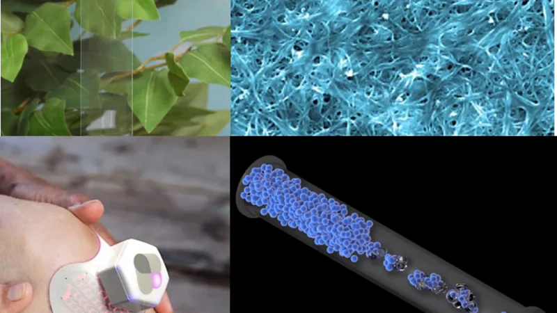
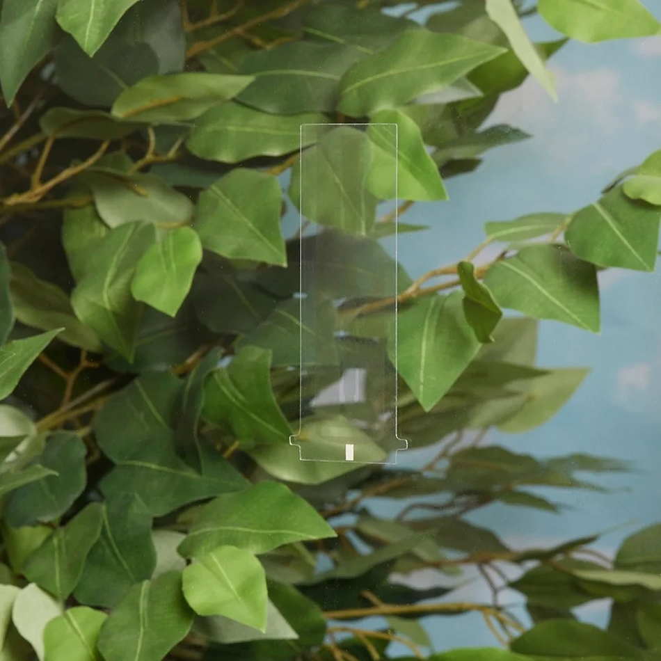
Transparent, flexible antennas
Today’s 5G frequencies don’t penetrate buildings well, and the need for more antennas to facilitate 5G speed is growing exponentially. The problem is that consumers don’t want unsightly features, like antennas, attached to their products or to be visible anywhere within their environments.
A new class of antenna is emerging to solve that problem. Transparent antennas, made with flexible, conductive hybrid films offering performance equivalents to leading low-loss, ceramic-based PCB laminates, work as well as traditional non-transparent printed antennas. They can be leveraged for automotive, cellular, NFC, Wi-Fi/Bluetooth, LPWAN, and GNSS/satellite use, to name a few.
 Join the free-to-attend online Festival on Printed Flexible Hybrid Electronics here
 Richard Morris, Director of Business Development, and the team at CHASM Advanced Materials believe that high-performance transparent antennas have the potential to overcome connectivity challenges in a variety of fields, including automotive, enterprise IoT and smart cities. These antennas can be easily integrated with glass or windows, providing a level of freedom that is hard to match. With peel-and-stick options, users can upgrade their connectivity setups without having to drill holes or risk damaging their assets. Furthermore, this technology can be integrated using various methods, such as OCA lamination and film insert molding processes.
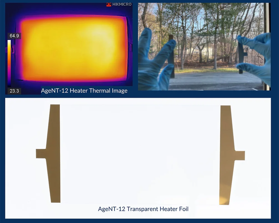
Transparent heaters
Our industry has long leveraged IME to carry electronic signals for heaters. Here at DuraTech, for example, we manufacture resistive heating elements to de-ice polycarbonate snowplow headlights. This is done by inserting a functional thin film printed with conductive silver ink into an injection molding tool so that it bonds with the resin of the molded lens. As a result, snowplow headlights that are illuminated with low heat producing LEDs stay free of snow and ice.
Companies like Chasm are taking that technology even further. For example, optical camera, LiDAR and radar sensors in advanced driving assistance systems (ADAS) don’t perform well in fog, rain snow and cold conditions. Yet, solutions like microwires or Indium-Tin-Oxide films can result in energy loss or distortion, thermal gradient issues or are easily cracked. CHASM’s AgeNT heaters are compatible with camera, lidar, and radar sensors, delivering rapid and uniform heating over the entire camera lens, lidome or radome surfaces. The heaters are also highly transparent, with no visible wires, and are highly stable during temperature, humidity and UV aging tests. Moreover, they are compatible with standard automotive voltage (12V), making them easy to integrate into existing vehicle systems. In comparison, other emerging technologies struggle to provide enough power density at 12V. AgeNT heaters can be mass-produced at low cost, making them an attractive solution for automotive manufacturers and suppliers.
The next step in transparent heater technology extends to road management systems. An example in development includes printed spherical heaters inserted into the compound curves of a toll system’s glass fisheye lenses. Sensors within these lenses must be able to operate in all weather conditions to identify vehicle size – from motor bikes to semi-trailers – to determine what toll rate applies to each vehicle. Another example is heaters for solar powered cameras placed at fixed road junctions to help municipalities and snow removal companies gauge road conditions. Armed with accurate information supplied by snow-, ice- and fog-free cameras, they can then determine how to mix the appropriate brine solutions and where to put them to keep roads safe for driving.
 Join us in Berlin -where the global printed electronics industry connects. Learn more here
 Cavitated inks
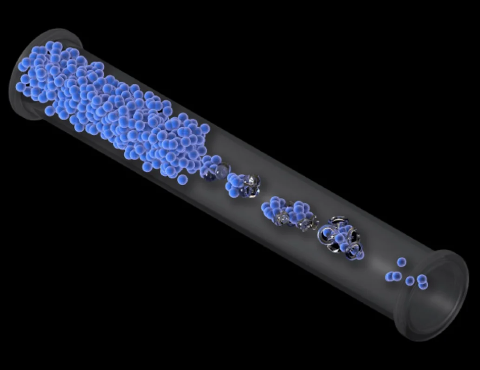
For most people, cavitation implies powerfully destructive liquid microjets and shock waves that will pit the hardest metals or ceramics. These are caused by significant pressure changes which form vacuum bubbles that collapse when the pressure is greater on the outside of the vacuum bubbles. One example is when a propeller turns in the water creating a pressure drop, thus forming the vacuum bubbles that ultimately collapse and pit the metal propeller. Today, however, cavitation is being leveraged in an entirely different way that’s rocking our industry.
A company called ACI Materials has developed a controlled cavitation process that produces functional inks with unparalleled nano particle dispersion – to less than .1 microns. Essentially, the process involves the controlled formation of vacuum bubbles within the material, and then fracturing the vacuum bubbles resulting in the release of energy. This energy is released in the form of liquid microjets and shock waves, creating the ultimate dispersion of the product mix and achieving near primary particle size (elimination of large agglomerates). Cavitation does not alter the morphology of malleable particles, although layered structures like graphite and nanoclays will exfoliate, forming high aspect ratio particles. The cavitation process creates ink with superior conductivity and mechanical performance, allowing printers to go places with a squeegee and a flood bar that we never could have imagined before. For example, they’re allowing printers to enter markets, like power management, that were formerly off-limits due to ink limitations.
The ACI Materials team has developed and currently produces the world’s only cavitated functional inks. ACI’s specially formulated inks enable solderability of silver-based additively manufactured printed circuits, allowing for high throughput, low cost, component attach in FHE applications. When this process is combined with a substrate such as PET, which is very low cost, printers can work toward a cost-comparative nanomaterials way to additively manufacture circuits – a huge benefit for them and the environment.
ACI’s Cavitation Process
Unlike current mixing methods, ACI’s patented cavitation process dramatically improves material performance, enabling new applications in Stretchable/Wearable Technology and Flexible Hybrid Electronics.
Cavitation also makes possible the ultra-fine dispersion of carbon nano materials. This matters in the manufacturing of stretchable fixed-resistance heaters, for instance. To consistently print a trace with a target resistance, the functional fillers, including carbon, must be fully dispersed. If they aren’t fully dispersed, the shearing forces of screen printing can continue to disperse the carbon fillers during the print run. This can result in a change in the resistance of each print over the course of the print run. Achieving full dispersion of carbon fillers is extremely difficult to do. Through cavitation, carbon is fully dispersed before it ever goes on the screen, resulting in consistently even output temperatures from fixed resistance heaters, even in print runs of thousands of heaters.
Ultimately, cavitated inks could make a tremendous difference to our personal carbon footprint. Cavitated ink, for example, can be used on stretchable material, enabling the creation of wearable heaters that conform to the human body – and that can withstand wash cycling and drying. So, if we can make a four-foot-long scarf with a printed heater that measures just 18 inches for the part of the scarf that wraps around your neck, how likely are you to turn up the heat in your home? Not very. It’s thin, flat, flexible, convenient, and extremely power efficient in more ways than one.
 Join us in Berlin -where the global printed electronics industry connects. Learn more here
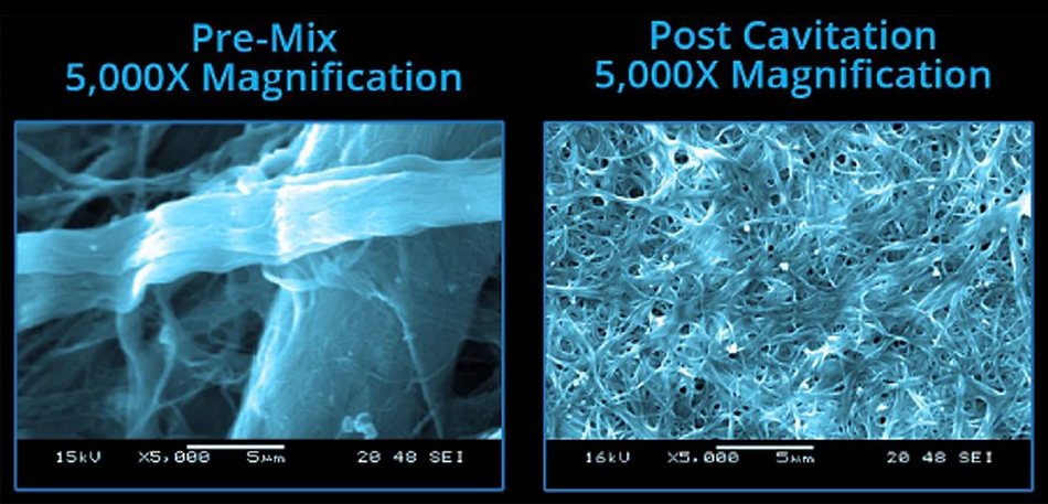
 The above SEM micrographs illustrate the ability of cavitation to untangle and disperse carbon nanotubes without destroying the nanotube walls. Cavitated inks also have a future in wearable medical technology such as heart rate and blood pressure monitors in the form of form-fitting shirts; brain sensors in the form of skull caps and printed wearable heaters for physical therapy.
Finally, cavitation itself is a green manufacturing process. Because it takes place in a closed stainless-steel environment, no VOCs are released (which also results in yields of nearly 100 percent).
More and more, OEMs are mandating that designers prove that we’re not contributing to the waste stream. If we can’t bring two or three environmentally sustainable options to the table that our customers can take to their boards of directors, we’ll lose the business. Medical manufacturing is a prime example, and this is where cavitation can also be a game changer.
Take glucose monitoring systems; millions of which are used daily. With cavitation, we can print those monitors using a tenth of a gram less silver per sheet to achieve the same signal strength. Not is only less silver ending up in landfills when those monitors are discarded, the monitors themselves will cost providers less. When you’re quoting the printing of 300 million glucose monitors in a year, we’re talking about significant cost savings and substantially less silver ending up in landfills. It’s where we’re headed today and where tomorrow absolutely must be.
Photobiomodulation
Wearable photobiomodulation (PBM) therapy is another new frontier for printed functional electronics. Previously known as low-level laser therapy, PBM is a medical treatment that applies low-level lasers or LEDs to the surface of a person’s body to relieve pain and accelerate the healing process. It’s a proven alternative to traditional treatments, such as opioids, for pain and inflammation. New applications promise benefits beyond tissue healing and pain reduction and include cosmetic applications for acne treatment and wrinkle reduction.
Not only do PBM wearable patches offer convenient, effective treatment for numerous medical conditions, but they are also non-invasive, making them safer for the patient than other medical treatments. They also don’t use harsh chemicals that can irritate skin the way that many acne treatments do, and they come with very little packaging – no bottles, no caps, or boxes that go directly into the waste stream.

Carewear's Light Therapy system is a wireless, wearable, over-the-counter FDA cleared, CE MDD class IIa medical device for the management of pain, treatment of soft tissue injury, wrinkles and acne. It is paired with a digital health infrastructure allowing clinicians to select treatment parameters and outcome indicators, monitor utilization and report real time through the cloud.
Implications
The examples we’ve looked at in this article are indicative of the central role functional printed electronics will have not only in the development of exciting new products that will improve our living standards, but also, by eliminating waste and scrap and allowing for resource-efficient material choices, in the future of additive manufacturing as it relates to environmental sustainability.
To keep our momentum going, it will be imperative that our industry actively promotes science, technology, engineering, and mathematics (STEM) education at every level and at every opportunity. The printed electronics industry isn’t alone in the search for skilled workers, and our competition continues to increase as technology permeates a growing number of employment sectors. In fact, the International Monetary Fund reports that by 2030, there will be a global shortage of more than 85 million tech workers, representing $8.5 trillion in lost annual revenue.
We are up to the challenge, though. The future of our industry is so exciting that it’s easy to share our enthusiasm: On a personal level, many of us are involved in local programs to promote STEM. Let’s keep that going; who knows where it can lead us next?
Michael has a background in engineering combined with leadership and business development in the digital and screen printing industry. Some of his projects have included the introduction of new manufacturing technologies at Hamilton Robotics, GE Medical, Medtronic Neurological, and Zoll Medical Corporation. As a founder and leader at Primary Image, Inc. in Reno, Nevada, a cutting-edge R & D organization, he and his team successfully launched several innovative solutions for companies in the gaming, military, governmental, and medical technology fields.
 Join the free-to-attend online Festival on Printed Flexible Hybrid Electronics here