Featured
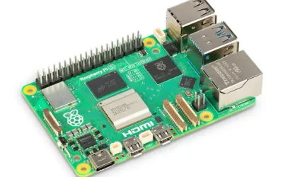
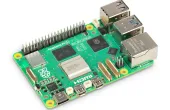
The Raspberry Pi Foundation just released their latest innovation, the Raspberry Pi 5.
This guide is written for engineers and technical teams building connected devices who need clear, field-ready guidance without getting lost in standards documentation.
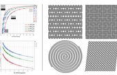
PCB Trace Width Calculator
The Raspberry Pi Foundation just released their latest innovation, the Raspberry Pi 5.
This comprehensive guide will cover the basics of PCB materials, the different types of materials available, their properties, and choosing the right material for your application.
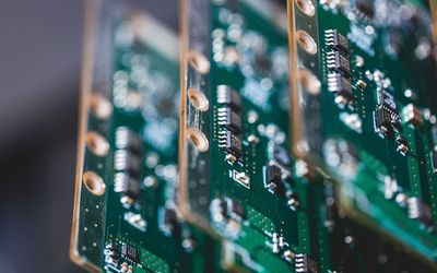
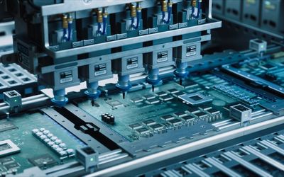
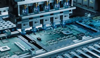
A Comprehensive Introduction to Flying Probe Test, its Essential Components, Advantages, Limitations, and Application Cases
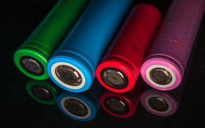
Understanding the key differences between the two high-in-demand battery types. This article focuses on Energy density, lifespan, safety, and cost trade-offs for the technical selection of Li-Ion and LiFePO4 batteries.
16 minutes read.
20 minutes read.
15 minutes read.
20 minutes read.
13 minutes read.
28 minutes read.

Electronics
Mouser Electronics is a worldwide leading authorized distributor of semiconductors and electronic components.
219 Posts
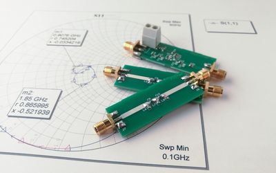
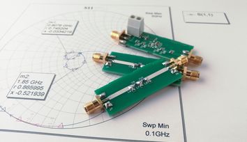
A guide covering the full radio-frequency design workflow, starting from setting specifications and choosing topologies to matching, simulation, layout, and verification, to help antenna engineers.
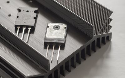
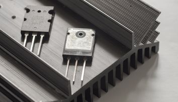
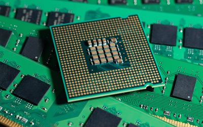
This article presents a detailed technical exploration of SiC MOSFET devices, covering material physics, device structure, switching behavior, and practical design considerations for high-efficiency power electronics systems.
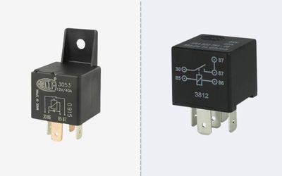
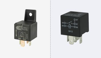
This article is a comprehensive technical guide to relay wiring diagrams, covering 4-pin and 5-pin configurations, working principles, safety practices, standards, and advanced relay applications in modern systems.
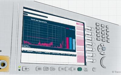
Explore how frequency shapes EMC behavior from RF emissions to ultra-low-frequency drift, with mitigation strategies for robust, compliant electronic system design.
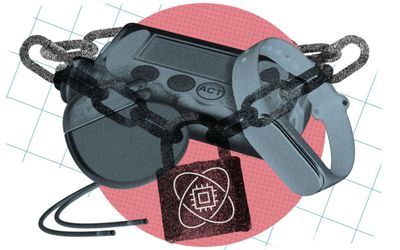
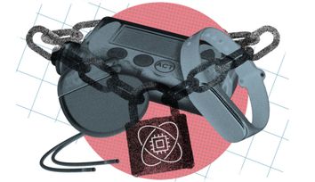
Ultra-efficient chip design enables extremely strong cryptography algorithms to run on energy-constrained edge devices.
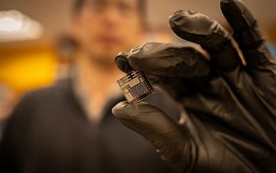
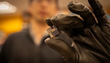
Researchers at ETH Zurich have now developed chip technology that enables verification of the authenticity of sensor data, including images or videos.
The integrated design achieves accurate micro gas chromatography and can help reduce the cost of monitoring chemical synthesis, natural gas pipelines or at-home air quality.
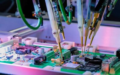
Hybrid bonding provides the adhesive free, copper to copper interconnects that are driving cutting edge 3D chip stacking. This article explains the theory, process, benefits, challenges, applications, and emerging trends of hybrid bonding for engineers.
The Raspberry Pi Foundation just released their latest innovation, the Raspberry Pi 5.
This comprehensive guide will cover the basics of PCB materials, the different types of materials available, their properties, and choosing the right material for your application.
A Comprehensive Introduction to Flying Probe Test, its Essential Components, Advantages, Limitations, and Application Cases
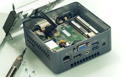
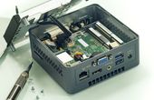
Discover the power of single-board computers for enhanced versatility and performance.
AI chips, designed for machine learning tasks, are spurring new chip architectures for efficient deep learning computation.

4 minutes read
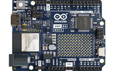
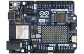
The new Arduino UNO R4 Wi-Fi board provides built-in Wi-Fi and Bluetooth communication as well as a 12×8 LED matrix display to give makers, hobbyists, and engineers an extremely versatile prototyping tool.
An examination of troubleshooting techniques for single board computer issues.
Kodak has a long history of manufacturing quality film products – starting with silver halide imaging films for consumers. Learn how Kodak is continuing that history, manufacturing a variety of industrial film products in many industries – from automotive to batteries to healthcare.

5 minutes read
In this episode, we unveil the astounding achievement of a student team that created an electric vehicle (EV) capable of shattering the 0-62mph speed record, leaving even the most capable state of the art supercars trailing behind.

16 minutes read
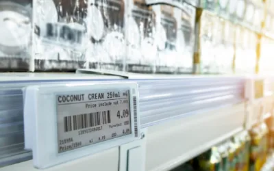
Electronic shelf labels (ESL) are connected, low-power ‘e-paper’ display devices that can replace traditional paper labels and can display text, numbers, icons, lines, barcodes and pictures. They enable retailers to automatically update individual shelf price labels from a central point across multiple stores and branches—or in certain geographic locations—at the touch of a button.

4 minutes read
MacroFab CEO Misha Govshteyn discusses the nuances of reshoring North American electronics manufacturing.

RISC-V, the groundbreaking open and customizable instruction set architecture (ISA), is transforming the world of microprocessors. Its exceptional flexibility empowers developers to craft processors precisely suited for their needs, setting it apart as the go-to choice for a diverse range of devices, from energy-efficient IoT gadgets to powerful servers.
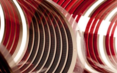
Organic Photovoltaics (OPV are a 3rd Gen PV technology with unique attribute. The key to their success is in Roll-to-Roll (R2R) processing. Here you will learn about the advantages and challenges of R2R manufacturing in OPVs and printed electronics
2 minutes read
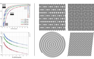
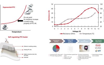
Heaters are one of the most successful applications of printed electronics. At first they seem deceptively simple, yet their successful realization is in fact an art relying on the interplay of all the elements from the right material selection to right design, right printing, etc. Learn how here.
6 minutes read
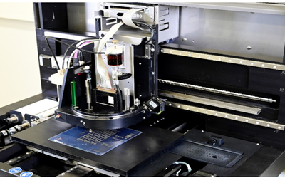
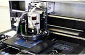
Advanced packaging of semiconductor-based sensors - specially on flexible substrates- brings very specific interconnection requirements. These often are related to a very narrow pitch of the interconnections or the fragility of the sensor. Learn how inkjet printing solves the issues
6 minutes read