Design for Manufacturability (DFM) in PCB Design: The Complete Guide
A PCB design can be electrically correct, pass every design rule check and perform exactly as expected on an engineer's screen - and still cause significant problems when it reaches manufacturing.

20 Oct, 2026. 10 minutes read
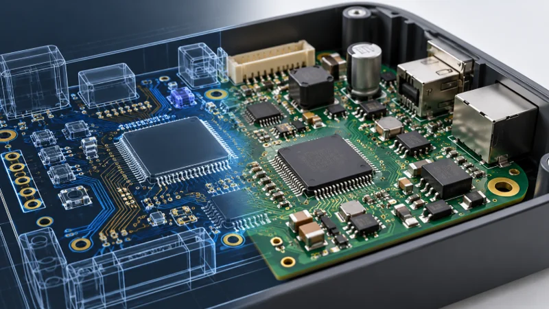
Placement is often approached primarily from an electrical perspective.
Signal integrity, routing length, power distribution and thermal performance are obviously important, but the assembly process also needs to influence where components are positioned.
Components placed extremely close together can restrict access for inspection and rework. Parts located too close to board edges may interfere with panelisation, depanelisation or assembly equipment.
Orientation matters too.
Consistent orientation of similar polarised components can reduce assembly and inspection errors. Clear polarity and pin-one identification also helps both automated inspection and manual troubleshooting.
Large or heavy components may require additional consideration because of the forces they experience during manufacturing and use.
Connectors deserve particular attention. Their position is frequently constrained by the finished product, yet they may also need mechanical support, adequate board-edge clearance and sufficient space for mating connectors.
Fiducials, tooling areas and test points should also be considered before every available piece of board area is filled.
The objective is not to make every board spacious. High-density designs are sometimes unavoidable.
The objective is to ensure that density exists because the product requires it, rather than because manufacturing requirements were considered too late.
A PCB design can be electrically correct, pass every design rule check and perform exactly as expected on an engineer’s screen - and still cause significant problems when it reaches manufacturing.
That is the gap Design for Manufacturability (DFM) is intended to close.
DFM means considering how a PCB will actually be fabricated, assembled, inspected and integrated into the finished product while the design is still being created. Rather than treating manufacturing as something that happens after design, it makes manufacturing constraints part of the design process itself.
The objective is not simply to produce a board that can be manufactured. Good DFM aims to produce a board that can be manufactured repeatedly, economically and reliably.
That distinction becomes increasingly important as a design moves from prototype to production.
1. What Is DFM in PCB Design?
Design for Manufacturability in PCB design is the practice of creating a board with the capabilities and limitations of real manufacturing processes in mind.
Every PCB fabrication and assembly process has tolerances. Copper features cannot be infinitely small. Drilled holes cannot be positioned with absolute precision. Solder paste does not deposit identically every time. Components, boards and mechanical parts all vary slightly within their specified tolerances.
A good PCB design accounts for these realities.
This means considering factors such as minimum trace spacing, drill sizes, annular rings, solder mask clearances, component spacing, assembly methods and mechanical constraints before manufacturing files are released.
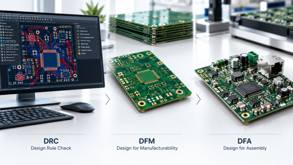
Importantly, DFM is not the same as simply running a Design Rule Check (DRC).
A DRC determines whether a design complies with a defined set of rules. DFM asks a broader question:
Can this design be manufactured reliably using the intended production process?
A board may pass DRC while still containing decisions that increase manufacturing cost, reduce yield or make assembly unnecessarily difficult.
DFM therefore needs to be considered as a design discipline rather than just a final software check.
2. Why DFM Should Start During PCB Design
One of the most expensive times to discover a design problem is after manufacturing has begun.
By that point, PCBs may already have been fabricated, components purchased, assembly scheduled and production capacity allocated. A relatively minor design change can then create delays across the entire project.
Many of these problems originate much earlier.
Component selection influences footprint geometry and assembly processes. Layer stack-up affects routing and fabrication. Component placement affects soldering, inspection and mechanical integration. Connector positioning can determine whether the finished board fits into its enclosure.
DFM is therefore most effective when it begins alongside the design rather than being applied after the design is supposedly finished.
This is particularly important when moving from prototypes to production.
An engineer may successfully assemble a handful of prototype boards despite small clearances, awkward component placement or difficult solder joints. At production volumes, however, small inefficiencies become repeatable manufacturing problems.
Good DFM reduces that risk by asking not only whether something is technically possible, but whether it is sensible to manufacture repeatedly.
3. PCB Fabrication Constraints Every Designer Should Understand
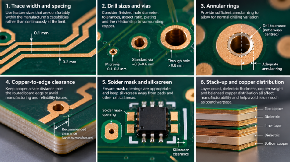
PCB fabrication involves several physical processes, each with its own tolerances and limitations.
Designers do not need to become PCB fabricators, but understanding the fundamentals helps avoid unnecessarily difficult or expensive designs.
Trace width and spacing
Very narrow traces and small copper-to-copper spacing can often be manufactured, but capability varies between fabricators and processes.
Using extremely fine features without a genuine electrical or density requirement can increase manufacturing complexity and potentially reduce yield.
Where space permits, designing comfortably within a manufacturer’s standard capabilities is generally preferable to designing continuously at the process limit.
Drill sizes and vias
Small drilled holes, particularly microvias and high-aspect-ratio vias, can introduce additional manufacturing requirements.
Designers should consider finished hole diameter, drill tolerance, board thickness, plating requirements and the relationship between the drilled hole and surrounding copper.
Annular rings
The annular ring is the copper surrounding a drilled hole.
Manufacturing tolerances mean the drill will not always land perfectly in the mathematical centre of the pad. Providing sufficient annular ring allows for normal drilling variation without compromising the connection.
Copper-to-edge clearance
Copper features positioned too close to a routed board edge can create manufacturing and reliability problems.
The required clearance depends on the fabrication method and board requirements, but board-edge constraints should be incorporated into the layout rather than checked only at release.
Solder mask and silkscreen
Solder mask openings must account for registration tolerances and the geometry of the pads they expose.
Silkscreen should also be kept away from exposed pads and other areas where printed markings could interfere with assembly.
Stack-up and copper distribution
Layer count, dielectric thickness, copper weight and controlled-impedance requirements all affect manufacturability.
Large imbalances in copper distribution can also contribute to problems such as board warpage.
The general DFM principle is straightforward: do not demand manufacturing precision unless the design actually requires it.
4. Designing PCB Footprints for Manufacturability
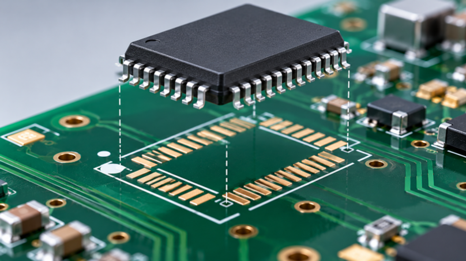
The footprint is where the electronic component meets the physical manufacturing process, which makes footprint accuracy fundamental to DFM.
A footprint is more than a collection of pads.
Pad dimensions, spacing, solder mask openings, paste apertures, courtyard definitions, polarity indicators and mechanical information can all influence whether a component can be assembled reliably.
Land patterns should reflect the component manufacturer’s recommendations, applicable standards and the intended assembly process.
Package dimensions also have tolerances. Designing around a single nominal dimension without considering allowable variation can create problems when components from different production batches are assembled.
Thermal pads require particular attention. Large exposed pads may require segmented solder paste apertures to control the amount and distribution of solder during reflow.
Courtyard information is also valuable because it helps designers maintain appropriate spacing between neighbouring components.
This is why using the correct CAD model matters. An inaccurate footprint can propagate a dimensional error directly into the manufactured board.
A schematic symbol error may cause an electrical problem. A footprint error can result in a component that simply cannot be soldered correctly to the PCB.
Both can stop a product, but the footprint is where the digital de
5. Component Placement for Reliable Manufacturing
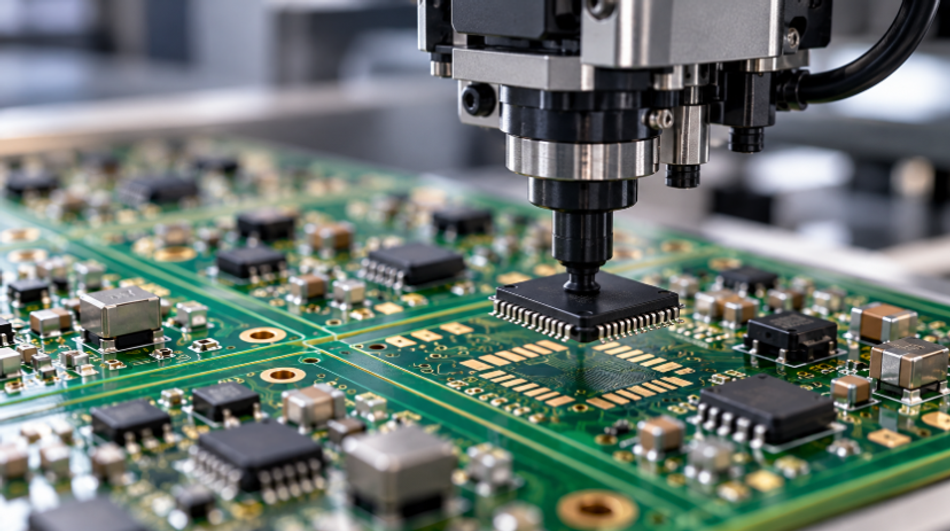
Placement is often approached primarily from an electrical perspective.
Signal integrity, routing length, power distribution and thermal performance are obviously important, but the assembly process also needs to influence where components are positioned.
Components placed extremely close together can restrict access for inspection and rework. Parts located too close to board edges may interfere with panelisation, depanelisation or assembly equipment.
Orientation matters too.
Consistent orientation of similar polarised components can reduce assembly and inspection errors. Clear polarity and pin-one identification also helps both automated inspection and manual troubleshooting.
Large or heavy components may require additional consideration because of the forces they experience during manufacturing and use.
Connectors deserve particular attention. Their position is frequently constrained by the finished product, yet they may also need mechanical support, adequate board-edge clearance and sufficient space for mating connectors.
Fiducials, tooling areas and test points should also be considered before every available piece of board area is filled.
The objective is not to make every board spacious. High-density designs are sometimes unavoidable.
The objective is to ensure that density exists because the product requires it, rather than because manufacturing requirements were considered too late.
6. Designing for PCB Assembly
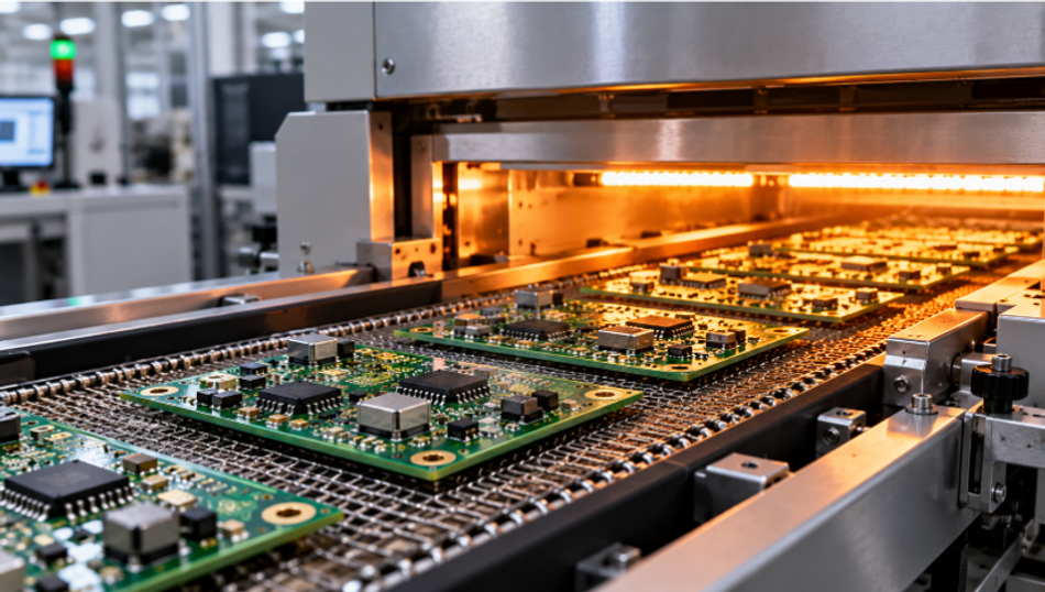
PCB fabrication produces the bare board. Design for Assembly (DFA) considers how components will then be attached to it.
The two disciplines are closely connected.
Surface-mount assembly typically involves solder paste printing, automated component placement and reflow soldering. Each stage introduces physical constraints.
Very small solder paste deposits, unsuitable pad geometries or uneven thermal behaviour can increase the likelihood of assembly defects.
Tombstoning is a familiar example. Small passive components can lift at one end during reflow when the forces created by solder wetting and temperature distribution become unbalanced.
Solder bridging can occur where pad spacing, paste deposition or component geometry makes unintended connections more likely.
Packages such as BGAs and QFNs create additional considerations because many or all solder joints are hidden underneath the component. Inspection methods, thermal pad design, via placement and rework capability therefore become more important.
Through-hole components can introduce different requirements, particularly where wave or selective soldering processes are used.
Testability and rework should also be considered.
A design that can be assembled but cannot be inspected, probed or repaired efficiently may create unnecessary production costs later.
DFM and DFA are therefore best viewed as overlapping disciplines: one ensures the board can be fabricated effectively, while the other ensures it can become a reliable assembled PCB.
7. Designing in 3D: Mechanical Fit Is Part of DFM
PCB design does not end at the board edge.
The assembled PCB normally exists inside a larger mechanical product containing an enclosure, mounting hardware, connectors, displays, switches, heatsinks, fans, cables and other physical parts.
This makes 3D mechanical verification an increasingly important part of PCB design.
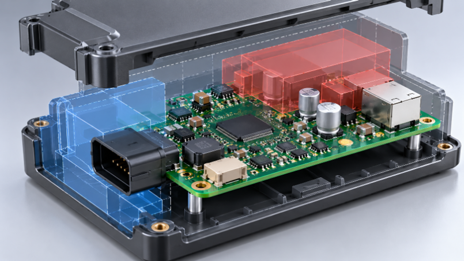
Accurate 3D CAD models allow engineers to represent the actual height and physical shape of components rather than treating the PCB purely as a two-dimensional layout.
This is particularly valuable for taller components such as connectors, electrolytic capacitors, transformers, heatsinks and switches.
The PCB assembly can then be evaluated against the surrounding mechanical design.
ECAD and MCAD collaboration allows potential collisions to be identified digitally: a capacitor touching an enclosure, a connector misaligned with an opening, a heatsink occupying the same space as a mechanical feature or a screw boss interfering with a component.
These are not necessarily PCB fabrication errors, but they are unquestionably manufacturing problems.
A board that can be fabricated perfectly but cannot be assembled into the final product has not been successfully designed for manufacture.
Accurate component 3D models are therefore more than visual aids. They allow mechanical clearance to become something that can be checked during the design process.
This becomes particularly powerful when the PCB and mechanical enclosure evolve together.
Instead of the ECAD engineer completing a PCB and throwing it over the wall to the mechanical team, both disciplines can work against a shared physical representation of the product.
That can remove an entire category of problems before physical prototypes are built.
8. Common PCB DFM Failures - and Why They Happen
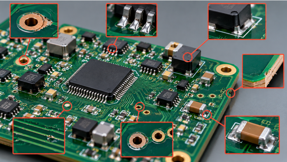
Many DFM problems are individually quite small.
The cost comes from discovering them late.
Common examples include:
Incorrect or unverified component footprints
Insufficient trace or copper clearances
Inadequate annular rings
Problematic drill or via requirements
Solder mask openings that are difficult to manufacture consistently
Silkscreen overlapping exposed pads
Components positioned too close together for reliable assembly or rework
Components placed too close to board edges
Poor thermal-pad or paste-mask design
Insufficient space for test access
Connector positioning that conflicts with the mechanical design
Component heights that interfere with the enclosure
Designs that unnecessarily use a fabricator’s minimum capabilities
What many of these failures have in common is not a lack of engineering knowledge. It is that one stage of the product development process has been considered without sufficient regard for the next.
DFM encourages engineers to think downstream.
Every important layout decision should consider what will eventually have to happen to that design physically.
9. Prototype vs Production: Designing for Scale
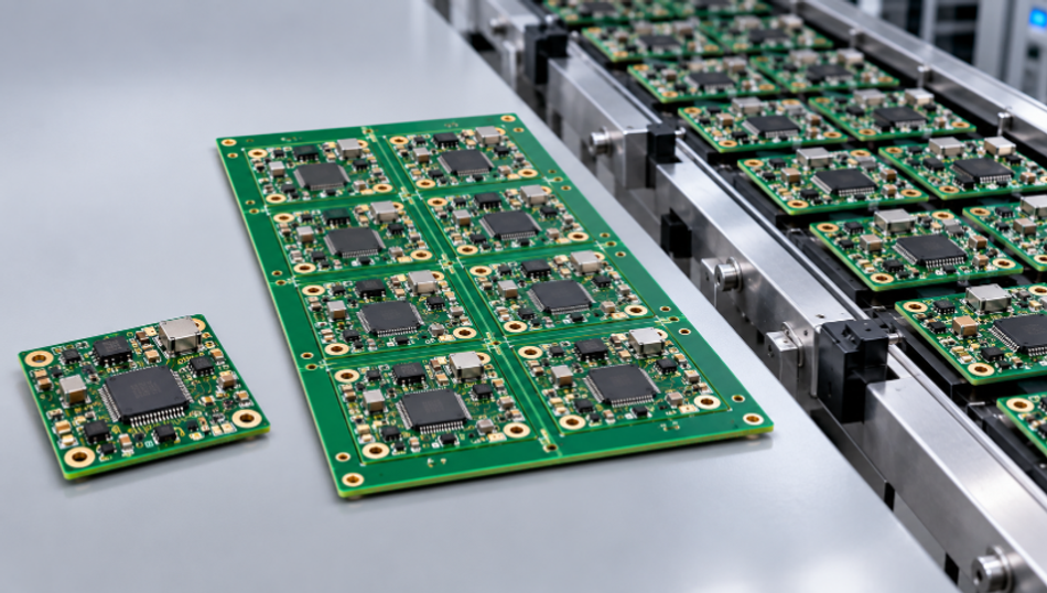
A successful prototype proves something important, but it does not automatically prove that a product is ready for volume manufacture.
Prototype quantities allow engineers and manufacturers to tolerate processes that would be undesirable at scale.
A technician may manually correct an awkward component on ten boards. Doing the same thing on 10,000 boards becomes a production problem.
This changes the way designers should think about tolerances.
A design that sits very close to manufacturing limits may produce acceptable prototypes but experience a lower yield once normal process variation appears across larger production quantities.
The same applies to assembly.
Component spacing, panelisation, test strategy, inspection and rework all become increasingly important as volume rises.
Production DFM therefore asks a slightly different question from prototype DFM:
Not simply, “Can we make this?”
But:
“Can we make this repeatedly, with predictable yield, quality and cost?”
That is an important distinction.
Good DFM creates margin where margin is inexpensive and reserves complexity for areas where the product genuinely needs it.
10. The PCB DFM Review: What to Check Before Release
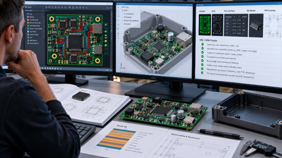
A structured DFM review should take place before manufacturing data is released.
The exact process varies according to the board and manufacturer, but several areas should normally be considered.
First, run the appropriate electrical and physical design-rule checks.
Then compare the design against the actual fabricator’s capabilities rather than relying entirely on generic design rules.
Review critical footprints against current component documentation, particularly unusual packages, connectors and components with exposed thermal pads.
Check component placement from an assembly perspective as well as an electrical one.
Review board-edge clearances, mounting holes, tooling requirements and other mechanical features.
Verify solder mask, paste mask and silkscreen information.
Review the manufacturing outputs themselves rather than assuming that because the PCB looks correct inside the design environment, the exported data must also be correct.
The mechanical assembly should then be checked in 3D where appropriate, including the enclosure, mounting hardware and any components with significant height or mechanical interaction.
Finally, apply engineering judgement.
Automated DFM tools are extremely valuable, but they evaluate the rules they have been given. They cannot always understand the design intent behind a product.
The strongest DFM process combines automated checking with an engineer who understands what is actually going to happen on the manufacturing line.
11. PCB DFM Checklist
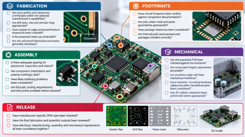
Before releasing a PCB for manufacture, designers should be able to answer the following questions:
Fabrication
Are trace widths and clearances comfortably within the selected manufacturer’s capabilities?
Are drill sizes, vias and annular rings appropriate?
Have copper-to-edge and board-feature clearances been checked?
Is the proposed stack-up achievable?
Are any advanced fabrication processes genuinely necessary?
Footprints
Have critical footprints been verified against component documentation?
Are pad, solder mask and paste geometries appropriate?
Have package tolerances been considered?
Are thermal pads and exposed-pad packages handled correctly?
Assembly
Is there adequate spacing for placement, inspection and rework?
Are component orientations and polarity markings clear?
Have likely soldering problems been considered?
Are fiducials, tooling requirements and test points available where required?
Mechanical
Has the populated PCB been checked against the enclosure?
Are component heights represented accurately?
Do connectors align with their mechanical interfaces?
Have heatsinks, mounting hardware, cables and other mechanical parts been considered?
Has 3D collision detection been performed where appropriate?
Release
Have manufacturer-specific DFM rules been checked?
Have the final fabrication and assembly outputs been reviewed?
Have electrical, manufacturing, assembly and mechanical requirements all been considered together?
A checklist cannot replace engineering judgement, but it can prevent simple omissions from becoming expensive manufacturing problems.
12. Conclusion: Good PCB Design Anticipates Manufacturing
The boundary between PCB design and PCB manufacturing is increasingly artificial.
The decisions that determine manufacturing success begin long before a fabricator receives the final production files.
They begin with component selection and footprints. They continue through routing, vias, stack-up and component placement. They extend into soldering, inspection and testing, and ultimately into the three-dimensional relationship between the assembled PCB and the mechanical product surrounding it.
That is why DFM should not be treated simply as a final check.
It is a way of designing.
The best PCB designers do not only ask whether the circuit will work or whether the layout will pass DRC. They consider how the board will be fabricated, populated, inspected, tested, fitted into its enclosure and reproduced at scale.
Modern CAD tools make more of that process visible before anything physical exists. Accurate footprints and 3D component models allow engineers to evaluate not only electrical connectivity but the physical reality of the product they are creating.
And that is ultimately what good Design for Manufacturability achieves.
It closes the gap between a PCB that works on screen and a product that can be built successfully in the real world.