Inkjet Printing for Advanced Manufacturing: PCBs, Flexible Electronics, Wearables & Beyond
Exploring the shift to additive digital printing in modern electronics fabrication.

20 Oct, 2026. 4 minutes read
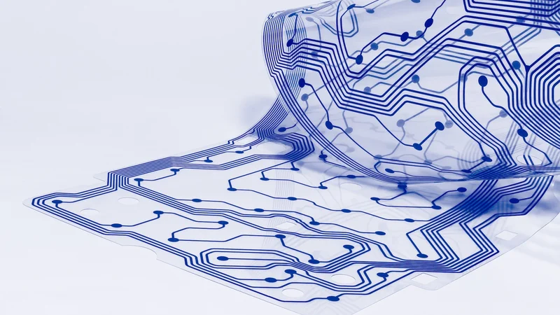
Electronics manufacturers face growing pressure to develop increasingly complex products while reducing production costs and development time. Shorter product lifecycles demand faster prototyping and frequent design changes. The current trend of wearables and flexible electronics has created demand for circuits that can be printed on non-rigid substrates.
Conventional PCB manufacturing involves multiple steps, including copper patterning, chemical etching, and drilling. Most of these processes end up increasing material waste, processing time and setup costs, especially during small production runs. They can also be difficult to adapt to flexible substrates and unconventional circuit designs.
Digital printing methods, such as inkjet printing, offer another way to produce electronic circuits. By depositing conductive materials directly onto substrates, these techniques can reduce material waste and simplify design iterations. They also give engineers greater flexibility to test new circuit layouts and work with different materials.
Moving Towards Additive Manufacturing with Selective Inkjet Printing
Rather than removing material from a coated substrate through processes such as etching, selective inkjet printing uses an additive approach. It deposits materials only where they are needed. This reduces material waste and simplifies pattern formation. Since ink droplets are deposited without direct contact with the substrate, the process is well suited for delicate and flexible materials that may be difficult to handle using conventional methods.
Engineers can also select inks based on their electrical and mechanical properties. For example, conductive inks can form circuit traces. On the other hand, protective inks can shield printed features from environmental exposure. By adjusting printing parameters, manufacturers can control pattern geometry and material deposition. This versatility makes selective inkjet printing a promising option for producing complex electronics with high efficiency and design flexibility.
Applying Inkjet Printing to Conventional PCB Manufacturing
The benefits of selective inkjet printing aren't limited to new types of substrates. This technology can also complement existing PCB manufacturing methods. Instead of replacing the entire fabrication process, selective inkjet printing can be introduced at specific stages to improve material deposition and pattern accuracy. For instance, inkjet printing can deposit etch-resistant ink onto selected areas of a copper layer to protect circuit traces. Inkjet printing can also apply solder mask around circuit features. It can make multiple passes to achieve the required thickness and coverage.
Additionally, multi-colour printing allows manufacturers to add component labels and identification marks to the board. By integrating selective inkjet printing into existing workflows, engineers can improve efficiency without modifying the process.
Beyond Traditional PCBs
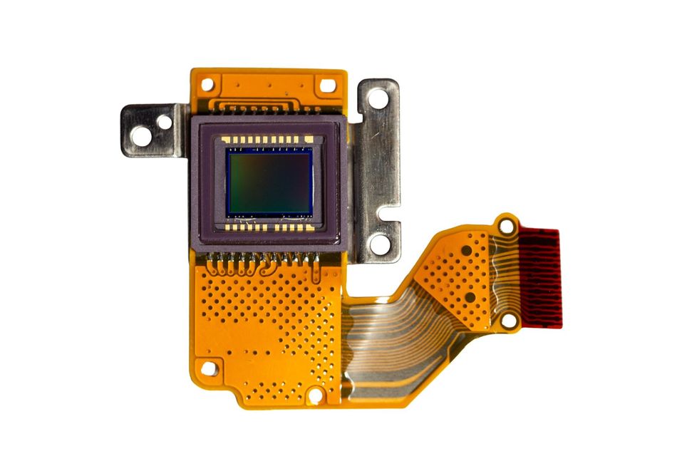
Selective inkjet printing allows engineers to create circuit patterns and features that are difficult to achieve with conventional rigid PCB processes. For instance, conductive inks can form electrical pathways directly on a substrate, which is useful in applications such as sensors and antennas.
Beyond that, selective inkjet printing can also be used to integrate electronics directly into components. It can deposit conductive or functional materials onto injection-molded parts and make the electronic features part of the product structure. Similarly, specialised inks can be deposited into recessed areas and cavities where conventional methods may struggle. These capabilities could help engineers develop compact and better-integrated electronic products.
Enabling Wearables, Displays, and Flexible Products
Inkjet printing can be ideal for consumer products or even industrial equipment where electronics need to follow the physical form of the product. This includes wearables, flexible displays, and industrial equipment with curved surfaces. This approach allows electronics to be designed around the product's geometry and functional requirements, rather than being limited by the rigid circuit board. For example, foldable devices such as the Samsung Galaxy Z Fold series and Apple’s iPhone Duo need to withstand repeated bending within a compact form factor. Of course, achieving reliable performance requires careful selection of inks and substrates to withstand repeated bending and environmental factors.
Engineering Advantages of Inkjet Manufacturing
From an engineering perspective, selective inkjet printing offers precise control over material deposition, pattern geometry, and other manufacturing parameters. As mentioned earlier, since the process deposits functional materials directly onto selected areas, it reduces material consumption compared to subtractive processes. It also reduces the need for etching chemicals and associated waste treatment.
Another advantage is the ability to control printed features through digital design files. Engineers can modify trace layouts, feature dimensions, or deposition patterns without significant tooling changes. Print resolution and layer thickness can also be managed by adjusting parameters to achieve the desired trace geometry and material coverage.
Why Inkjet Printing Could Open New Manufacturing Markets
This technology could help manufacturers explore applications that require unconventional form factors and specialised circuit designs. Similarly, in-mould electronics could enable manufacturers to integrate electronics directly into components.
Selective inkjet printing can also improve radio-frequency components and interactive surfaces. Printed antennas could support wireless communication, while conductive patterns on product surfaces could enable touch-sensitive controls. As ink formulations and printhead technology continue to advance, selective inkjet printing could become a go-to option for bringing new designs from prototype to production.
Conclusion
Inkjet printing can complement conventional PCB manufacturing while opening up new possibilities in flexible, wearable, and functional electronics. Its digital control, selective material deposition, and ability to work with different functional inks make it useful for customised designs, rapid prototyping, and small-batch production.

If you're looking to improve flexibility and efficiency in your electronics manufacturing process, visit the Industrial Print Integration (IPI) conference, taking place on 24-25 November 2026 in Neuss, Germany. The event will focus on exploring the technologies shaping printed electronics.