What Is a Semiconductor? Band Gap, Doping, Materials, and Devices
A semiconductor is a material whose electrical conductivity falls between that of a conductor and an insulator and can be controlled by temperature, light, and impurities. This article covers semiconductor materials, doping, diodes, transistors, and integrated circuits.

12 Oct, 2026. 26 minutes read

Silicon wafer and semiconductor technology underpinning modern data processing and electronic systems.
This article was first published on
www.wevolver.comKey Takeaways
A semiconductor is a material whose electrical conductivity falls between that of a conductor and an insulator and can be controlled by temperature, light, electric fields, and the introduction of impurities.
The band gap determines how readily a semiconductor generates mobile charge carriers. Silicon has a band gap of about 1.12 eV at room temperature, while gallium arsenide is about 1.42 eV; wider-band-gap materials such as silicon carbide and gallium nitride support higher-temperature and higher-power applications.
Doping deliberately introduces small concentrations of impurities into a semiconductor to control its carrier concentration. Donor dopants produce n-type semiconductors, where electrons are the majority carriers, while acceptor dopants produce p-type semiconductors, where holes are the majority carriers.
Silicon remains the dominant semiconductor material for microprocessors, memory, integrated circuits, and many photovoltaic applications. Materials such as silicon carbide (SiC) and gallium nitride (GaN) extend semiconductor technology into high-voltage, high-frequency, and high-temperature power electronics.
Semiconductor materials are fabricated into diodes, transistors, and integrated circuits (ICs) through processes such as doping, deposition, etching, and lithography. A chip is a packaged or unpackaged semiconductor die containing a functional electronic circuit; the semiconductor material itself is not synonymous with the finished device.
What Is a Semiconductor?
A semiconductor is a material whose electrical conductivity can be controlled over a useful range by changing its temperature, illumination, electric field, or concentration of impurity atoms. Its conductivity is generally lower than that of a conductor and higher than that of an insulator, but this intermediate position is not what makes semiconductors technologically important. Their value comes from the ability to precisely control the concentration and movement of charge carriers.
At the atomic scale, semiconductor behavior is governed by the material's electronic band structure. The valence band contains electrons bound to atoms, while the conduction band contains energy states in which electrons can move through the crystal and contribute to electric current. The energy difference between these bands is the band gap. In a semiconductor, the gap is small enough that external energy can generate mobile charge carriers, while still large enough to permit useful control over conductivity.
When an electron gains sufficient energy to cross the band gap, it leaves behind a vacancy in the valence band. This vacancy behaves as a positively charged carrier called a hole. Temperature and light can generate electron-hole pairs naturally, while controlled doping introduces impurity atoms that increase either electron or hole concentrations. These mechanisms allow engineers to tailor the electrical properties of semiconductor materials for specific devices.
This controllability distinguishes semiconductors from conventional conductors and insulators:
Property | Conductor | Semiconductor | Insulator |
Electrical conductivity | Very high. | Controllable over a wide range. | Very low. |
Band structure | Partially filled bands or overlapping valence and conduction bands. | Valence and conduction bands separated by a relatively small band gap. | Large band gap. |
Primary charge carriers | Predominantly free electrons. | Electrons and holes. | Very few mobile carriers under normal conditions. |
Response to temperature | Conductivity generally decreases as temperature rises. | Conductivity generally increases as temperature rises. | Remains very low under ordinary conditions. |
Examples | Copper, aluminum, and silver. | Silicon, germanium, gallium arsenide, SiC, and GaN. | Glass, ceramics, polymers, and diamonds. |
Typical applications | Power transmission and electrical interconnections. | Diodes, transistors, sensors, memory, processors, and power devices. | Electrical isolation and dielectric layers. |
Silicon illustrates the principle well. At 298 K, intrinsic silicon has an electron concentration of approximately:
nᵢ ≈ 1.0 × 10¹⁰ cm⁻³
This is many orders of magnitude lower than the free-electron concentration in a typical metal. Yet silicon's carrier concentration can be changed dramatically through doping, enabling precise control of its electrical conductivity. This is the foundation of semiconductor device engineering.
Modern electronic devices exploit this control in different ways. A semiconductor junction can be engineered to form a diode that controls current flow, while carefully structured semiconductor regions form transistors that switch or amplify electrical signals. Millions or billions of these devices can then be fabricated together to create integrated circuits (ICs) and modern microprocessors.
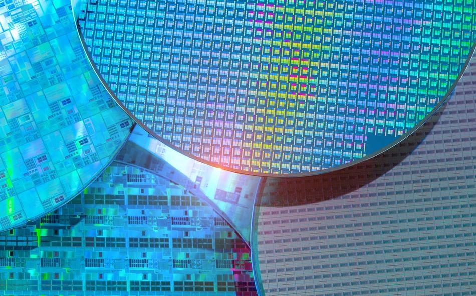
The resulting technology underpins smartphones, computers, communications equipment, vehicles, medical systems, industrial controls, and data centers. Global semiconductor sales reached $791.7 billion in 2025, according to the Semiconductor Industry Association, demonstrating the scale of the industry supporting this technology.
How Semiconductors Work: Energy Bands and the Band Gap
The electrical behavior of a semiconductor begins with its electronic structure. In crystalline silicon, each atom forms covalent bonds with four neighboring atoms by sharing its four valence electrons. When many atoms form an ordered crystal lattice, their individual atomic energy levels interact and split into closely spaced ranges of allowed energies called energy bands.
The highest occupied band at absolute zero is the valence band. Above it lies the conduction band, whose electrons can move through the crystal and contribute to electric current. The energy difference between the two is the band gap, represented by E_g.
E_g = E_c - E_v
where:
E_g = band-gap energy
E_c = conduction-band edge
E_v = valence-band edge
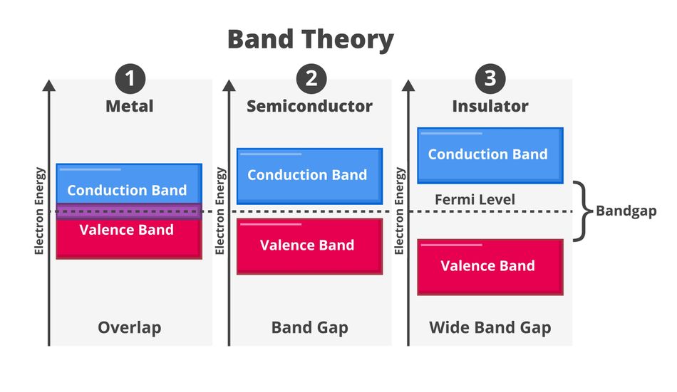
The band gap represents a range of energies in which allowed electronic states are absent in the ideal crystal. Its magnitude determines how readily electrons can be excited from the valence band into the conduction band by thermal energy, photons, or other forms of excitation.
In a conductor, occupied and available electronic states overlap, or a relevant band is partially filled, allowing electrons to respond readily to an applied electric field. In an insulator, the band gap is large enough that very few electrons can be thermally excited into conducting states under ordinary conditions. A semiconductor has a smaller band gap, allowing its carrier population and electrical conductivity to be controlled through temperature, light, doping, and external fields.
Electrons and Holes
At absolute zero, an intrinsic semiconductor has a filled valence band and an essentially empty conduction band. As temperature increases, thermal energy excites a small fraction of electrons across the band gap. Each excited electron becomes a mobile conduction-band carrier and leaves an unoccupied state in the valence band.
This vacancy is called a hole. A hole is not a physical particle; it is an effective positive charge carrier that represents the collective movement of valence-band electrons. When a neighboring electron moves into a hole, it leaves a new vacancy behind, causing the hole to appear to move through the crystal.
Both electrons and holes contribute to electrical conduction:
Electrons move through available states in the conduction band.
Holes represent the net movement of positive charge through the valence band.
Under an applied electric field, these carriers acquire a net drift velocity. The resulting conductivity depends on both carrier concentration and mobility:
σ = q(nμ_n + pμ_p)
where:
σ = electrical conductivity
q = elementary charge
n = electron concentration
p = hole concentration
μ_n = electron mobility
μ_p = hole mobility
This relationship is central to semiconductor engineering. Increasing the concentration of electrons or holes can substantially increase conductivity, while changes in mobility affect how efficiently those carriers move through the crystal. Doping provides the primary means of deliberately controlling carrier concentration.
Light can also generate charge carriers. When a semiconductor absorbs a photon with energy equal to or greater than its band gap, the photon can promote an electron into the conduction band and create an electron-hole pair. This mechanism is fundamental to photovoltaic cells and photodetectors and is also related to light generation in semiconductor optoelectronic devices.
Band Gap and Intrinsic Carrier Concentration
The band gap has a strong influence on the number of thermally generated carriers in an intrinsic semiconductor. A commonly used approximation for intrinsic carrier concentration is:
n_i = √(N_c N_v) × exp(-E_g / 2kT)
where:
n_i = intrinsic carrier concentration
N_c = effective density of states in the conduction band
N_v = effective density of states in the valence band
E_g = band-gap energy
k = Boltzmann constant
T = absolute temperature
Because E_g appears in the exponential term, relatively small differences in band-gap energy can produce large differences in intrinsic carrier concentration.
Material | Band gap at approximately 300 K (eV) | Intrinsic carrier concentration, n_i (cm⁻³) |
Germanium (Ge) | 0.66 | ~2.4 × 10¹³ |
Silicon (Si) | 1.12 | ~1.0 × 10¹⁰ |
Gallium arsenide (GaAs) | 1.42 | ~2 × 10⁶ |
Germanium has a narrower band gap than silicon, so thermal excitation produces substantially more intrinsic carriers at the same temperature. Gallium arsenide has a wider band gap and consequently a much lower intrinsic carrier concentration. These values are temperature-dependent and can vary with the material parameters and models used.
For comparison, metals typically have carrier concentrations on the order of 10²²–10²³ cm⁻³. Their electronic structure, however, differs fundamentally from that of intrinsic semiconductors. The relatively low intrinsic carrier concentration of a semiconductor is therefore only one part of its engineering significance.
Doping allows manufacturers to introduce controlled concentrations of donor or acceptor impurities, increasing the number of majority carriers and tailoring electrical conductivity. This control is what enables semiconductor materials to be engineered into the junctions and active regions used in diodes, transistors, sensors, memory, and integrated circuits.
Recommended reading: Bandgap Voltage Reference: Complete Guide for Analog Engineers
Intrinsic vs. Extrinsic Semiconductors
An intrinsic semiconductor is a highly pure semiconductor in which the electrical behavior is determined primarily by the material itself rather than intentionally introduced dopants. At thermal equilibrium, electrons and holes are generated in pairs, so their concentrations are equal:
n = p = n_i
where:
n = electron concentration
p = hole concentration
n_i = intrinsic carrier concentration
Pure silicon is the standard example. At room temperature, its intrinsic carrier concentration is about 1.0 × 10¹⁰ cm⁻³, leaving relatively few mobile carriers compared with a metal.
An extrinsic semiconductor is intentionally modified through doping, in which controlled concentrations of impurity atoms are introduced into the crystal. The dopants alter the carrier concentration and therefore the material's electrical conductivity. Depending on the dopant, the semiconductor becomes either n-type or p-type.
Property | Intrinsic semiconductor | Extrinsic semiconductor |
Composition | High-purity host crystal | Host crystal containing controlled dopant atoms |
Carrier balance | n = p = n_i | Majority and minority carriers occur in unequal concentrations |
Majority carrier | Neither; electrons and holes are equal | Electrons in n-type; holes in p-type |
Carrier concentration | Determined primarily by temperature and band gap | Controlled primarily through doping, with temperature also affecting carrier behavior |
Electrical conductivity | Relatively low at room temperature | Can be increased substantially through controlled doping |
Typical example | Undoped silicon | Phosphorus-doped or boron-doped silicon |
The distinction between the two types is fundamental to semiconductor engineering. Doping does not simply make a material “more conductive”; it gives engineers control over the type and concentration of charge carriers. This control allows different regions of the same crystal to be engineered with different electrical properties and joined to form semiconductor junctions.
N-Type and P-Type Semiconductors
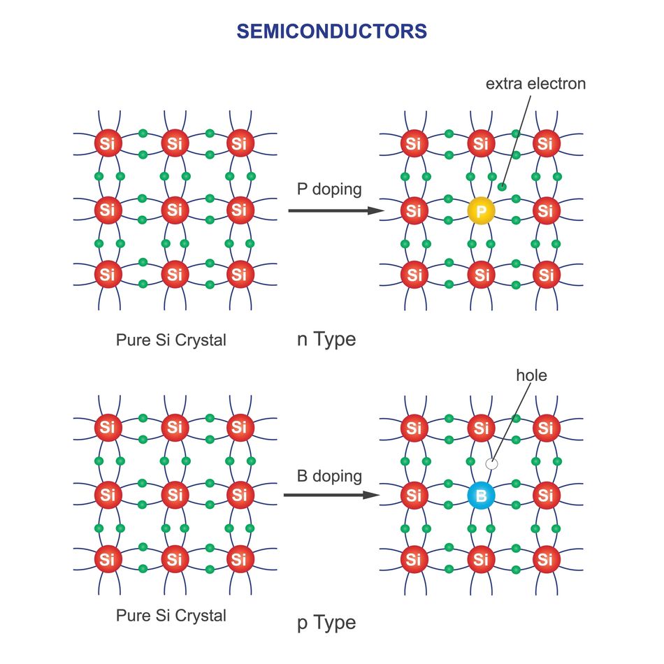
An n-type semiconductor is produced by introducing donor atoms that contribute additional electrons to the crystal. In silicon, phosphorus is a common donor because it has five valence electrons. Four participate in covalent bonds with neighboring silicon atoms, while the fifth is weakly bound and can become a conduction electron.
A p-type semiconductor is produced using acceptor atoms such as boron, which has three valence electrons. When boron replaces a silicon atom in the lattice, one covalent bond lacks an electron. The resulting vacancy behaves as a mobile hole.
In both cases, the dopant concentration can be engineered to control the semiconductor's electrical properties. Electrons are the majority carriers in n-type material, while holes are the majority carriers in p-type material; the opposite carrier remains present as the minority carrier.
Worked Example: What 1 ppm of Dopant Does to Silicon
A very small dopant concentration can produce a large change in carrier concentration. Consider silicon doped with phosphorus at 1 part per million (ppm).
Silicon contains approximately 5 × 10²² atoms per cm³.
A concentration of 1 ppm corresponds to a fraction of 10⁻⁶. Therefore, the phosphorus concentration is:
N_D = (5 × 10²² cm⁻³)(10⁻⁶)
N_D = 5 × 10¹⁶ cm⁻³
If the phosphorus donors are effectively ionized and compensation is negligible, the electron concentration is approximately equal to the donor concentration:
n ≈ N_D
n ≈ 5 × 10¹⁶ cm⁻³
Intrinsic silicon at approximately room temperature has an electron concentration of about:
n_i ≈ 1.0 × 10¹⁰ cm⁻³
The increase in electron concentration relative to intrinsic silicon is therefore:
n / n_i ≈ (5 × 10¹⁶) / (1.0 × 10¹⁰)
n / n_i ≈ 5 × 10⁶
Thus, 1 ppm of phosphorus can increase the equilibrium electron concentration by roughly five million times under these simplified conditions. The increase in electrical conductivity is not necessarily the same factor because carrier mobility generally decreases as dopant concentration increases.
This example illustrates why doping is so powerful: an impurity concentration of only one atom per million host atoms can fundamentally change the electrical behavior of a semiconductor.
N-Type vs. P-Type Semiconductors: How Doping Works
Doping replaces a small fraction of host atoms with impurity atoms that have a different number of valence electrons. In silicon, the difference determines whether the dopant contributes electrons or creates conditions for holes to become the dominant charge carriers.
N-Type Semiconductors
Silicon is a Group 14 element with four valence electrons, allowing each atom to form four covalent bonds with neighboring silicon atoms. When a small fraction of silicon atoms is replaced with a Group 15 element such as phosphorus, the dopant has five valence electrons.
Four electrons participate in covalent bonding with neighboring silicon atoms. The fifth is only weakly bound to the phosphorus atom and can be thermally excited into the conduction band. In silicon, donor binding energies are typically on the order of hundredths of an electronvolt, far below the 1.12 eV band gap of intrinsic silicon at room temperature.
The phosphorus atom therefore acts as a donor, supplying an additional conduction electron. The resulting material is an n-type semiconductor, in which electrons are the majority carriers, and holes are the minority carriers. Arsenic is another common donor dopant used in silicon.
P-Type Semiconductors
For p-type material, silicon can be doped with a Group 13 element such as boron, which has three valence electrons rather than silicon's four. The boron atom can form three complete covalent bonds, but the fourth bond lacks an electron.
A neighboring valence-band electron can occupy this incomplete bond, leaving an unoccupied state that behaves as a mobile positive charge carrier—a hole. The boron atom therefore acts as an acceptor.
The resulting material is a p-type semiconductor, in which holes are the majority carriers and electrons are the minority carriers. Aluminum can also serve as an acceptor dopant in silicon.
Property | N-type | P-type |
Dopant type | Donor | Acceptor |
Typical silicon dopants | Phosphorus, arsenic | Boron, aluminum |
Valence-electron difference | One extra electron | One fewer electron |
Majority carriers | Electrons | Holes |
Minority carriers | Holes | Electrons |
Dopant energy level | Donor level near conduction band | Acceptor level near valence band |
The distinction between n-type and p-type material is not simply a difference in conductivity. It determines which carrier dominates electrical transport, how semiconductor junctions behave, and how devices such as diodes and transistors are engineered. By placing n-type and p-type regions next to one another, manufacturers can create controlled junctions that form the basis of many semiconductor devices.
Carrier Mobility
Electrons and holes also differ in how efficiently they move through a semiconductor. Carrier mobility, measured in cm²/V·s, describes how strongly a carrier responds to an applied electric field.
For silicon at room temperature, electron mobility is approximately 1,500 cm²/V·s, while hole mobility is approximately 500 cm²/V·s under low-field conditions. Thus, electrons generally have about three times the mobility of holes in silicon.
This difference matters when comparing n-type and p-type device performance. Higher electron mobility can enable faster carrier transport and lower resistive losses in appropriately designed n-type regions, while p-type regions remain essential because semiconductor devices depend on controlled combinations of both carrier types.
Recommended reading: N-Type Vs P-Type: Difference Between P-Type and N-Type Semiconductors
The P-N Junction: Where Semiconductor Devices Begin
When p-type and n-type regions are formed next to each other within the same semiconductor crystal, they create a p-n junction. This interface is the fundamental building block of many semiconductor devices, including diodes, solar cells, photodetectors, and transistor structures.
Immediately after the junction forms, electrons from the n-type region diffuse toward the p-type region, where they recombine with holes. Similarly, holes diffuse toward the n-type side and recombine with electrons. This diffusion leaves behind fixed, ionized donor atoms on the n side and acceptor atoms on the p side.
The resulting region near the junction contains very few mobile charge carriers and is called the depletion region. The fixed ions within this region create an internal electric field that opposes further diffusion of majority carriers. At equilibrium, diffusion and electric-field-driven drift balance each other, producing a built-in potential across the junction.
The behavior of this junction changes when an external voltage is applied:
Forward bias: A positive voltage is applied to the p side relative to the n side. The external field reduces the junction's potential barrier and narrows the depletion region, allowing majority carriers to cross the junction more readily. Current therefore increases rapidly with applied voltage.
Reverse bias: A negative voltage is applied to the p side relative to the n side. The potential barrier increases, and the depletion region widens, strongly suppressing majority-carrier flow. A small reverse leakage current remains because of minority carriers and other physical mechanisms.
If the reverse voltage becomes sufficiently large, the junction can undergo breakdown, producing a sharp increase in reverse current. The breakdown voltage depends on factors such as dopant concentration, junction structure, semiconductor material, and device design. Depending on the device, breakdown can occur at voltages ranging from a few volts to several kilovolts.
The rectifying behavior of the p-n junction—allowing substantial current in one direction while strongly restricting it in the other—is the operating principle of a diode. More complex structures extend this concept by combining multiple semiconductor regions. For example, p-n-p and n-p-n structures form the basis of bipolar junction transistors, while carefully engineered p-type and n-type regions are also used throughout integrated circuits and power semiconductor devices.
The p-n junction therefore marks the transition from controlling carrier concentration through doping to using that control to perform a specific electrical function.
Semiconductor Materials: Silicon, Germanium, and Compound Semiconductors
Semiconductor materials can be broadly divided into elemental semiconductors, made from a single element, and compound semiconductors, formed from two or more elements. Silicon (Si) and germanium (Ge) are elemental semiconductors, while gallium arsenide (GaAs), gallium nitride (GaN), and indium phosphide (InP) are compound semiconductors.
Material selection depends on more than band gap alone. Carrier mobility, thermal conductivity, breakdown field, electron saturation velocity, optical properties, defect density, and the quality of interfaces with insulating materials all influence which semiconductor is appropriate for a given device.
Silicon
Silicon has remained the dominant semiconductor material because it combines a useful band gap with strong thermal stability, mature manufacturing processes, and excellent material and interface properties.
One of its greatest advantages is the high-quality silicon dioxide (SiO₂) that can be formed directly on its surface. This insulating layer is critical to technologies such as metal-oxide-semiconductor field-effect transistors (MOSFETs), where it enables precise control of the semiconductor channel.
Silicon also has a band gap of approximately 1.12 eV at room temperature and can be manufactured at extremely high levels of purity. Decades of process development have made silicon compatible with large-scale wafer fabrication, advanced lithography, and highly integrated electronic circuits. Silicon therefore dominates applications ranging from microprocessors and memory to power devices and photovoltaic cells.
Germanium
Germanium was central to the earliest development of semiconductor electronics. In December 1947, researchers at Bell Labs demonstrated the first working transistor using high-purity germanium.
Germanium has a smaller band gap than silicon—approximately 0.66 eV at room temperature. Its intrinsic carrier concentration is therefore much higher, which contributes to greater leakage current as temperature increases. This thermal behavior was one of the major reasons silicon became preferable for most mainstream semiconductor applications.
Germanium has not disappeared from semiconductor technology. Its high carrier mobility and compatibility with certain compound-semiconductor and silicon-based structures make it useful in specialized applications, including high-speed electronics, infrared optics, and research devices.
Compound and Wide-Bandgap Semiconductors
Compound semiconductors provide material properties that silicon cannot always match. Gallium arsenide (GaAs), for example, has higher electron mobility than silicon and strong optoelectronic properties, making it useful in high-frequency electronics, lasers, LEDs, and other photonic applications.
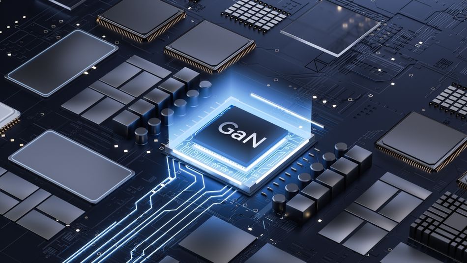
Wide-bandgap (WBG) semiconductors form another important class. Silicon carbide (SiC) and gallium nitride (GaN) have band gaps of approximately 3.3 eV and 3.4 eV, respectively, compared with about 1.12 eV for silicon. Their wider band gaps are associated with high critical electric fields and the ability to operate at higher temperatures and voltages.
These properties make SiC and GaN important in power electronics, where reducing conduction and switching losses can improve efficiency and reduce system size. SiC is well suited to high-voltage applications such as electric-vehicle traction inverters, industrial power conversion, and grid-connected systems. GaN is increasingly used for high-frequency power conversion, compact chargers, RF electronics, and other applications where fast switching is valuable.
Material | Classification | Band gap at ~300 K (eV) | Representative applications |
Silicon (Si) | Elemental | 1.12 | Microprocessors, memory, integrated circuits, power devices, solar cells |
Germanium (Ge) | Elemental | 0.66 | Infrared devices, specialized high-speed electronics, research |
Gallium arsenide (GaAs) | III-V compound | 1.42 | RF electronics, lasers, LEDs, optoelectronics |
Silicon carbide (SiC) | Wide-bandgap compound | 3.3 | High-voltage power electronics, EV inverters, industrial power conversion |
Gallium nitride (GaN) | Wide-bandgap compound | 3.4 | High-frequency power conversion, RF electronics, LEDs |
Indium phosphide (InP) | III-V compound | ~1.34 | Fiber-optic communications, photonics, high-speed electronics |
The choice among these semiconductor materials is therefore an engineering trade-off. Silicon remains difficult to replace where manufacturing maturity, cost, integration density, and the Si/SiO₂ interface are decisive. Compound and wide-bandgap materials become more attractive when high frequency, high voltage, high temperature, optical performance, or switching efficiency is the dominant requirement.
Recommended reading: Silicon Semiconductor: A Comprehensive Guide to Silicon and its Use in Semiconductor Technology
Semiconductor Devices: From Diodes to Microprocessors
Semiconductor materials become useful electronic components when carefully doped and structured into devices that control, generate, detect, store, or process electrical signals. These devices range from simple two-terminal components to microprocessors containing billions of transistors.
The Semiconductor Industry Association (SIA) broadly groups semiconductor products into six categories:
Category | Primary function |
Discrete | Performs a basic electronic function as an individual component |
Optoelectronics | Generates or detects light |
Sensors and actuators | Detects physical conditions or converts electrical signals into physical action |
Analog | Processes continuously varying signals such as voltage, temperature, sound, and light |
Memory | Stores digital data or instructions |
Logic | Performs computation, control, and digital signal processing |
These categories can overlap within a single device. A system-on-chip (SoC), for example, can integrate logic, memory, analog circuits, and other functions on one semiconductor die.
Diodes
A diode is a two-terminal semiconductor device that controls current primarily through the behavior of a junction. The conventional p-n junction diode conducts readily under forward bias and strongly restricts current under reverse bias until breakdown occurs.
Different diode structures provide different functions. Rectifier diodes convert alternating current to pulsating direct current, while Zener and avalanche diodes exploit controlled breakdown for voltage regulation and protection. Photodiodes convert incident light into electrical signals, and light-emitting diodes (LEDs) convert electrical energy into light through radiative recombination.
LEDs illustrate how semiconductor materials can be selected for specific electronic and optical properties. Gallium nitride (GaN) and related III-nitride materials are widely used for blue and other short-wavelength LEDs because their wide band gaps support the required photon energies.
Solar cells use the complementary process: photons absorbed by the semiconductor generate electron-hole pairs, and the device structure separates these carriers to produce an electrical output.
Recommended reading: How Does a Diode Work: Unraveling the Heart of Electronic Control
Transistors
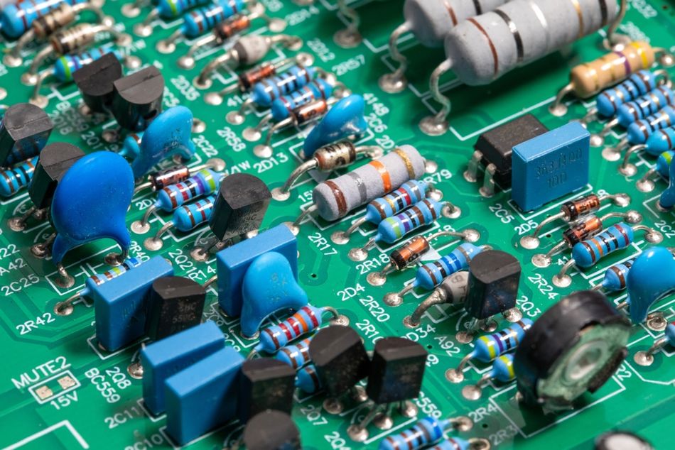
A transistor is a semiconductor device used primarily for switching or amplification. Unlike a diode, which has two terminals, a transistor uses an additional control terminal to regulate current through the device.
In a bipolar junction transistor (BJT), a small base current controls a much larger collector-emitter current. This current gain allows the transistor to amplify signals and operate as a switch.
A metal-oxide-semiconductor field-effect transistor (MOSFET) controls current differently. An applied voltage at the gate creates or modifies a conductive channel between the source and drain. Because the insulated gate draws very little steady-state current, MOSFETs can provide efficient voltage-controlled switching and amplification.
The first successful transistor demonstration took place at Bell Labs in December 1947. John Bardeen and Walter Brattain demonstrated amplification using two closely spaced gold contacts on high-purity germanium. William Shockley subsequently developed the junction-transistor concept. Bardeen, Brattain, and Shockley shared the 1956 Nobel Prize in Physics for their work on semiconductors and the discovery of the transistor effect.
Recommended reading: How Does a Transistor Work? Theory & Practical Applications for Engineers
Integrated Circuits and Microprocessors
An integrated circuit (IC) combines many semiconductor devices and passive elements on a single piece of semiconductor material. Transistors provide switching and amplification, while resistive, capacitive, and interconnect structures perform additional circuit functions.
During fabrication, many copies of an IC are formed simultaneously across a semiconductor wafer. The wafer is then separated into individual dies, which are packaged and connected to the outside world.
The development of the IC transformed electronics by replacing assemblies of individually wired components with densely integrated electronic circuits. Jack Kilby and Robert Noyce are widely recognized as key pioneers of integrated-circuit technology. Kilby demonstrated an early integrated circuit at Texas Instruments in 1958, while Noyce developed a practical monolithic IC approach at Fairchild Semiconductor based on planar processing and integrated metal interconnections.
Miniaturization and Moore's Law
The continuing reduction in transistor dimensions has driven semiconductor miniaturization for decades. Smaller transistors allow more devices to fit onto a single die, increasing computational capability while improving performance, power efficiency, or both when supported by advances in circuit and system design.
In 1965, Gordon Moore observed that the number of components on integrated circuits was increasing rapidly and projected that the number would approximately double over a period of about one to two years. The observation became known as Moore's Law and became a useful description of the industry's historical scaling trend.
Modern microprocessors and system-on-chip devices contain billions of transistors. Achieving this density requires advances not only in transistor design but also in materials, lithography, interconnects, power management, and packaging.
The progression from a single p-n junction to billions of interconnected transistors illustrates the central principle of semiconductor engineering: precisely controlling charge carriers at microscopic scales makes it possible to build increasingly complex electronic systems on a tiny piece of material.
Recommended reading: Miniaturization of Components: Enabling Next-Generation Medical Devices and Implantables
Semiconductor vs. Chip: What Is the Difference?
“Semiconductor,” “chip,” and “integrated circuit” are often used interchangeably in everyday language, but they describe different things in semiconductor engineering. A semiconductor is a material, while a chip is a fabricated piece of semiconductor containing one or more electronic circuits or devices.
Term | What it means | Example |
Semiconductor | A material whose electrical properties can be controlled through factors such as doping, temperature, light, and electric fields | Silicon, gallium nitride |
Wafer | A thin, precisely manufactured semiconductor substrate on which many devices or circuits are fabricated simultaneously | 300 mm silicon wafer |
Die / microchip | An individual piece cut from a processed wafer, containing a fabricated semiconductor device or circuit | Processor die, memory die |
Integrated circuit (IC) | An electronic circuit containing multiple interconnected devices and components fabricated on a common substrate | Microprocessor, memory IC |
Discrete semiconductor | An individual semiconductor device designed to perform a specific function | Diode, power MOSFET, bipolar transistor |
Package | The physical enclosure and electrical interface that protects a die and connects it to a circuit board or system | QFN, BGA, power module |
The distinction becomes clearer when following the manufacturing sequence. A semiconductor wafer provides the starting substrate. Through processes such as doping, deposition, etching, and lithography, manufacturers form transistors, diodes, interconnects, and other structures across the wafer. The wafer is then divided into individual dies, which can be tested and assembled into packages.
An integrated circuit describes the functionality fabricated on the die, whereas the die refers to the physical piece of semiconductor containing that circuit. Once packaged, the component can be mounted onto a printed circuit board and connected to other electronic components.
This distinction also explains why not every semiconductor device is a microchip in the conventional sense. A discrete diode or transistor is fabricated from semiconductor material and may contain a single primary device structure, while a modern microchip can contain billions of interconnected transistors and other circuit elements.
In short:
Semiconductor = material
Wafer = substrate used for fabrication
Die = individual piece cut from the wafer
IC = integrated electronic circuit fabricated on the die
Package = protected, externally connectable form of the die
The terms overlap in everyday usage, but keeping these distinctions clear is important when discussing semiconductor manufacturing, electronic components, and modern microchips.
Recommended reading: Chips and Wafers: What's the Difference?
How Semiconductor Chips Are Made
Manufacturing an integrated circuit involves hundreds of tightly controlled process steps that transform a polished semiconductor wafer into patterned electronic devices. The sequence combines doping, deposition, lithography, etching, oxidation, cleaning, and thermal processing to build transistors and the interconnect structures that connect them.
The process begins with a highly purified semiconductor wafer, typically silicon. Manufacturers repeatedly deposit or grow thin material layers, pattern selected regions with lithography, remove unwanted material through etching, and introduce dopants where specific electrical properties are required. These steps gradually construct transistor structures and the insulating and conducting layers surrounding them.
Lithography transfers circuit patterns onto a light-sensitive material called photoresist. In advanced fabrication, extreme ultraviolet (EUV) lithography uses light with a wavelength of 13.5 nm to pattern extremely small features. EUV systems operate at different numerical apertures: conventional EUV systems use a numerical aperture of 0.33, while newer High-NA EUV systems use 0.55 to enable finer patterning. Lithographic resolution is one factor in determining achievable feature dimensions, but final transistor dimensions also depend on process integration, materials, patterning techniques, and device architecture.
A simplified fabrication sequence is:
Wafer preparation: A high-purity semiconductor crystal is sliced into wafers and polished to create an extremely flat surface.
Layer formation: Conducting, insulating, and semiconductor materials are deposited or grown on the wafer.
Lithography: A patterned exposure defines where subsequent processing will occur.
Etching: Selected portions of a material layer are removed according to the lithographic pattern.
Doping: Controlled impurities are introduced into selected semiconductor regions to establish n-type and p-type electrical characteristics.
Repetition: These processes are repeated many times to construct transistors and multilayer interconnects.
Testing and dicing: Electrical testing identifies defective dies before the wafer is separated into individual dies.
Packaging and assembly: Functional dies are mounted, electrically connected, protected, and packaged so they can be integrated into an electronic system.
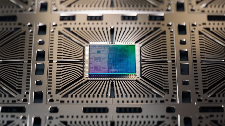
Because thousands of dies can be fabricated simultaneously on a single wafer, semiconductor manufacturing relies on exceptional control of contamination, temperature, pressure, material thickness, alignment, and defect density. A defect at the wrong location can render an individual die unusable, making process control and yield critical to manufacturing economics.
The completed die is not yet a finished electronic product. Packaging provides mechanical protection, thermal management, and electrical connections between the die and the outside system. Advanced packaging can also place multiple dies or functional chiplets within a single package, allowing system-level performance to improve without relying solely on further transistor miniaturization.
Recommended reading: Semiconductor Fabrication Process: The Ultimate Guide to Creating Cutting-Edge Electronics
Where Semiconductors Are Used
Semiconductors are the foundation of modern electronic systems because their electrical properties can be engineered for switching, amplification, sensing, light generation, energy conversion, and data storage. Their applications extend from individual electronic components to infrastructure that supports computing, communications, transportation, and energy systems.
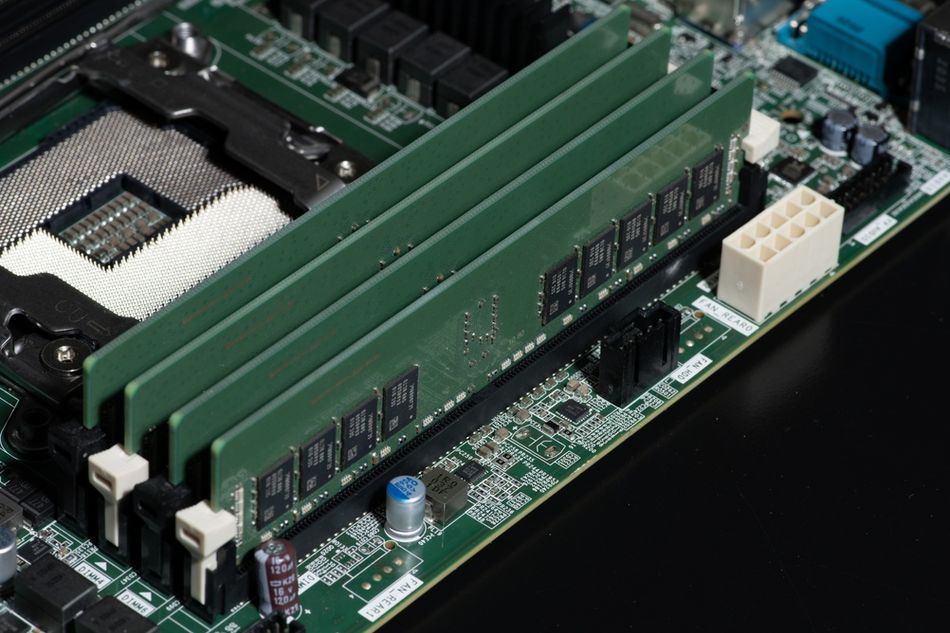
Computing and communications: Transistors form the switching elements in microprocessors, memory, networking equipment, and communications hardware. Modern smartphones, computers, servers, and data centers depend on highly integrated semiconductor devices to process, store, and transmit information. Continued miniaturization has increased computing capability while improving energy efficiency at the device and system levels.
Power electronics and power management: Semiconductor switches and diodes control the conversion and distribution of electrical energy in power supplies, electric vehicles, industrial equipment, renewable-energy systems, and consumer electronics. Wide-bandgap materials such as silicon carbide (SiC) and gallium nitride (GaN) can support higher switching frequencies, voltages, and temperatures than conventional silicon devices. Higher switching frequency can also reduce the size of passive components such as inductors and capacitors, enabling more compact power-conversion systems.
Energy generation and conversion: Semiconductor devices are central to photovoltaic systems, where solar cells convert light into electrical energy. Power semiconductor devices then regulate and convert that electricity for storage, transmission, or use by electrical loads. SiC devices are increasingly important in high-voltage power conversion, including solar inverters and electric-vehicle powertrains.
Lighting and optoelectronics: Semiconductor materials can convert electrical energy into light or convert light into electrical signals. GaN-based materials enable LEDs across much of the visible spectrum, while GaAs and other III-V compounds are used in lasers, photodetectors, and other optoelectronic systems.
Sensing and control: Semiconductor sensors detect physical and chemical conditions such as temperature, pressure, acceleration, magnetic fields, light, and gas concentration. These devices provide the inputs needed for automotive systems industrial automation, medical equipment, consumer electronics, and other cyber-physical systems.
The breadth of these applications comes from the same underlying principle developed throughout this article: semiconductor properties can be precisely controlled. Doping determines carrier concentration, junctions control current flow, transistors provide switching and amplification, and integrated circuits combine billions of devices into increasingly complex systems.
As electronic systems become more connected and energy-intensive, advances in semiconductor materials, transistor architectures, lithography, and packaging will continue to shape computing performance, power efficiency, communications, and automation.
Common Misconceptions and Engineering Trade-Offs
Understanding semiconductor technology requires more than knowing how electrons move through a crystal. Engineers must balance electrical performance, temperature, materials, manufacturing complexity, reliability, and system-level cost. Several common assumptions can obscure those trade-offs.
“Semiconductor” means silicon.
Silicon is the dominant material for integrated circuits, but it is not the only semiconductor that matters. Gallium arsenide (GaAs) offers useful high-frequency and optoelectronic properties, while gallium nitride (GaN) and silicon carbide (SiC) provide advantages in high-frequency and high-power applications. Material selection depends on the requirements of the device rather than on a single measure of performance.Temperature is a secondary consideration.
Semiconductor properties are strongly temperature-dependent. As temperature increases, intrinsic carrier concentration generally rises, which can increase leakage current and alter device behavior. Germanium's relatively small band gap contributes to greater temperature sensitivity than silicon. Device specifications must therefore be evaluated across the actual operating temperature range, not only at room temperature.A wider band gap is always better.
Wide-bandgap materials can provide high breakdown fields, high-temperature operation, and fast switching, but these advantages do not eliminate engineering constraints. Substrate quality, defects, thermal management, manufacturing complexity, packaging, and material cost can all affect the practical value of a WBG device. A material that performs better at the device level may not produce the lowest-cost or most efficient system in every application.Doping simply adds more carriers.
Doping increases the concentration of the desired majority carriers, but higher dopant concentrations can also increase impurity scattering and reduce carrier mobility. Because conductivity depends on both carrier concentration and mobility, increasing the number of carriers does not produce a proportional increase in conductivity.The semiconductor with the highest device performance is automatically the best choice.
Semiconductor selection is a system-level decision. Engineers must weigh electrical characteristics against thermal performance, reliability, manufacturability, packaging, availability, and total system cost. The optimal material is the one that meets the application's requirements with an appropriate balance of these factors.
The central engineering lesson is that semiconductor technology is not about maximizing a single property. It is about controlling material properties precisely enough to achieve the required electrical function while managing the physical and economic constraints of the complete device and system.
Conclusion
A semiconductor is a material whose electrical conductivity can be precisely controlled. Its electronic band structure determines how easily charge carriers can be generated, while temperature, light, electric fields, and doping provide mechanisms for controlling those carriers.
Doping illustrates how dramatically small changes in composition can alter electrical behavior. Under simplified room-temperature conditions, adding phosphorus to silicon at a concentration of 1 part per million can produce a donor concentration of approximately 5 × 10¹⁶ cm⁻³—about five million times the intrinsic carrier concentration of silicon. The resulting n-type or p-type material provides the controlled carrier populations needed to build semiconductor devices.
Combining n-type and p-type regions creates p-n junctions, whose rectifying behavior forms the foundation of diodes and many more complex devices. Transistors extend this control to switching and amplification, while integrated circuits combine billions of transistors and other components into microprocessors, memory, sensors, and other electronic systems.
Silicon remains the dominant semiconductor platform because of its balanced electrical properties, thermal behavior, manufacturing maturity, and high-quality silicon dioxide interface. Germanium, gallium arsenide, gallium nitride, and silicon carbide remain important where their electrical, optical, or thermal properties provide advantages over silicon.
For engineers, semiconductor selection ultimately comes down to requirements: band gap, carrier mobility, breakdown field, operating temperature, switching frequency, voltage, thermal performance, manufacturing constraints, and system cost. Understanding these relationships is what turns semiconductor physics into practical electronic engineering.
Frequently Asked Questions
What is a semiconductor in simple terms?
A semiconductor is a material whose electrical conductivity can be controlled. It generally conducts less readily than a metal such as copper but more readily than an electrical insulator. Temperature, light, electric fields, and controlled impurities can change its carrier concentration and conductivity, making semiconductor materials useful for electronic devices.
What are examples of semiconductors?
Common elemental semiconductors include silicon (Si) and germanium (Ge). Important compound semiconductor materials include gallium arsenide (GaAs), silicon carbide (SiC), gallium nitride (GaN), silicon germanium (SiGe), and indium phosphide (InP). Different materials are selected according to properties such as band gap, carrier mobility, thermal performance, and optical response.
What is the difference between a semiconductor and a chip?
A semiconductor is a material. A chip or die is a fabricated piece of semiconductor containing one or more electronic devices or integrated circuits. Multiple dies are produced from a wafer, tested, separated, and packaged before being incorporated into electronic systems.
Why is silicon the most widely used semiconductor?
Silicon combines a useful band gap, good thermal properties, abundant raw material, mature manufacturing processes, and a high-quality silicon dioxide interface. That combination makes silicon highly effective for integrated circuits, memory, power devices, and photovoltaic cells.
What is the difference between intrinsic and extrinsic semiconductors?
An intrinsic semiconductor is undoped or negligibly doped, so its carrier population is determined primarily by the material's own electronic structure and thermal excitation. At equilibrium, electron and hole concentrations are equal:
n = p = n_i
An extrinsic semiconductor has intentionally introduced dopants that change its carrier concentration. Electrons become the majority carriers in n-type material, while holes become the majority carriers in p-type material.
Is a semiconductor a conductor or an insulator?
Neither. A semiconductor has electronic properties distinct from both conductors and insulators. Its conductivity can vary substantially with temperature, illumination, electric fields, and doping. This controllability—not simply its intermediate conductivity—is what makes semiconductors useful in electronics.
How do semiconductors work in electronic devices?
Engineers create controlled regions of different carrier types within semiconductor materials. P-n junctions form the basis of diodes and other devices, while transistors use electrical signals or electric fields to control current. Integrated circuits combine large numbers of these devices to perform computation, store information, amplify signals, and control electronic systems.
What does doping do to a semiconductor?
Doping introduces controlled concentrations of impurity atoms into a semiconductor crystal to alter its carrier concentration. In silicon, donor dopants such as phosphorus provide additional electrons and produce n-type material, while acceptor dopants such as boron promote hole conduction and produce p-type material. Even very small dopant concentrations can change electrical conductivity by several orders of magnitude.
References
[1] Toshiba Electronic Devices & Storage Corporation, “What is a semiconductor?” Toshiba Electronic Devices & Storage Corporation. [Online]. Available: https://toshiba.semicon-storage.com/us/semiconductor/knowledge/e-learning/discrete/chap1/chap1-1.html
[2] U.S. Department of Energy, “Solar photovoltaic cell basics,” U.S. Department of Energy. [Online]. Available: https://www.energy.gov/cmei/systems/solar-photovoltaic-cell-basics
[3] Semiconductor Industry Association, “What are semiconductors?” Semiconductor Industry Association. [Online]. Available: https://www.semiconductors.org/semiconductors-101/what-are-semiconductors/
[4] OpenStax, “9.7 Semiconductor devices,” in University Physics Volume 3, OpenStax. [Online]. Available: https://openstax.org/books/university-physics-volume-3/pages/9-7-semiconductor-devices
[5] U.S. Department of Energy, “Wide bandgap semiconductors for power electronics,” Quadrennial Technology Review 2015, Technology Assessment 6N. [Online]. Available: https://www.energy.gov/sites/default/files/2016/02/f29/QTR2015-6N-Wide-Bandgap-Semiconductors-for-Power-Electronics.pdf
[6] Computer History Museum, “1947: Invention of the point-contact transistor,” Computer History Museum, The Silicon Engine. [Online]. Available: https://www.computerhistory.org/siliconengine/invention-of-the-point-contact-transistor/
[7] ASML, “EUV lithography systems,” ASML. [Online]. Available: https://www.asml.com/en/products/euv-lithography-systems
[8] Semiconductor Industry Association, “Global annual semiconductor sales increase 25.6% to $791.7 billion in 2025,” Feb. 6, 2026. [Online]. Available: https://www.semiconductors.org/global-annual-semiconductor-sales-increase-25-6-to-791-7-billion-in-2025/
in this article
1. Key Takeaways2. What Is a Semiconductor?3. How Semiconductors Work: Energy Bands and the Band GapIntrinsic vs. Extrinsic SemiconductorsN-Type vs. P-Type Semiconductors: How Doping Works6. The P-N Junction: Where Semiconductor Devices Begin7. Semiconductor Materials: Silicon, Germanium, and Compound Semiconductors8. Semiconductor Devices: From Diodes to MicroprocessorsSemiconductor vs. Chip: What Is the Difference?10. How Semiconductor Chips Are Made11. Where Semiconductors Are Used12. Common Misconceptions and Engineering Trade-Offs13. Conclusion14. Frequently Asked Questions