PCB Panelization: Everything You Need to Know
PCB Panelization is a PCB manufacturing technique. It involves the grouping of several small printed circuit boards to form a single array, which is known as a panel. Panelization is commonly employed in PCB manufacturing because it saves time and cost. This article discusses the conditions, design considerations, methods, types, and benefits of PCB panelization.

09 Feb, 2023. 11 minutes read
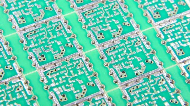
Panelized PCB
Introduction
PCB panelization is a manufacturing technique where smaller circuit boards are produced in bulk and joined to one another to form a single array. This bulk production fosters the easy movement of PCBs through an assembly line. The individual boards can easily be depanelized or removed from the array for packaging or installation into products.
CNC (Computer Numerical Control) machines are utilized in PCB production and assembly facilities. These CNC machines can design PCBs that are rather large in size. But typically, electronic products use small-sized PCBs. Therefore, several copies of the PCB design are given to the CNC machine to fully leverage its capability. This process of producing multiple PCBs on a single board is called PCB Panelization and the resulting board spread is known as a PCB Panel. [1]
PCB Panelization is the most commonly used PCB manufacturing technique, as it saves both time and cost.
What is a PCB Panel?
A PCB panel, also known as a PCB array or PCB matrix, is one board made up of several separate boards. A single array of smaller PCBs is created by integrally connecting them all. Following assembly, the panel is divided into separate PCBs during the breakout process, which is known as depanelization. Each board in the array can be easily separated or removed for packaging or installation into products.
Defects are reduced as a result of the printed circuit board panelization process since automated assembly machines frequently run into less issues during assembly. The panel may feature a single design or a variety of designs. The panel is single-up if there is just one piece or board, and multi-up if there are more. By increasing PCB material utilization, panelization lowers PCB cost and speeds up automated PCB assembly, with less cost. Panels are typically applied to high-volume PCB production.
When is PCB Panelization Required?
The CNC machines used to manufacture PCBs consume virtually the same amount of power for small-sized PCBs as it does for large-sized boards. So for small-sized PCB designs, multiple copies can be made efficiently, as it is replicated over the panel, with only a slight price increase. The PCB order in product design often falls between ten to hundred thousand.
PCB panels are used in these situations to save cost and time. Additionally, certain PCBs are too small to meet SMT fixture requirements, therefore mounting them on a big board enhances manufacturing convenience. The yield of fabrication is increased and quality control is made easier with automated production. Also, automatic machines can execute the SMT process for many PCBs simultaneously, increasing the utilization rate of the equipment. [2]
Combinations of PCB Panelization
PCB panels usually need to adopt a structure. However, there are many ways to design the panels. Selecting one can be sometimes difficult because it needs to be determined by considering the density and distribution of components on the board as well as the configuration of equipment. Nevertheless, all types of panels have their advantages and disadvantages. Some panelization combinations are discussed below:
ABCD Combination
This combination is usually applied by PCB companies as they combine all single PCB orders on a PCB Panel to save time and cost. There are various benefits to this form of panelization. First of all, it is appropriate for the manufacturing model involving various PCB combinations in products like toys and home appliances. Also, it helps to increase production efficiency and minimize costs, which can significantly lower stock levels of semi-finished goods and enable manufacturers to meet customers' demands for quick shipping.
However, there are drawbacks to this panelization method as well. One is the issue of product differentiation on an assembly line being challenging to control, thereby resulting in product confusion. Moreso, if one board in the combination is of poor quality fewer panelizations will be made overall, which is bad for general manufacturing. The 3 combination types are presented below:
AAAA Combination
This type of combination panelization is the most commonly-used panelization method. Its popularity is a result of many benefits. First off, there is no need to scrutinize conditions specific to SMT manufacturers' fabrication processes or product combinations here, as it is compatible with all. Moreover, order panelization is unaffected by production numbers, allowing the most panels possible based on the highest number of SMT equipment, which results in the best level of manufacturability out of all possible panelization combinations.
Furthermore, the influence of the pad orientation of specific components during the printing of the stencil design process will not cause a reduction in printing quality. Finally, because of the changing panel orientations in each run of the entire method, operating difficulty won't accumulate.
ABAB Combination
This combination is typically employed in designing PCBs for medium-sized electronic products such as calculators and handheld devices. In this case, around 3 to 5 small PCB designs are used, which are interfaced together in the final product. This combination is therefore suitable for designing multiple PCBs of a single product. However, it is much less applied than the preceding two. [3]
Depanelization Methods
Depanelization is the separation of individual circuit boards from the PCB panel or array. It can be carried out in different ways:
V-Score Panelization
This popular panelization technique divides individual PCBs using V-shaped grooves. By applying an angled blade, these grooves roughly remove a third of the board's thickness from the top and bottom of the board. Given that the remaining third of the board between the grooves is surprisingly sturdy and that hand-breaking might inflict stress on the PCB and other close components, a machine is frequently utilized to complete the breakout operation.
Design Considerations for V-Score Panelization
To be assured of the PCB panel’s feasibility, the following design considerations should be accounted for while performing V-Score panelization.
Irregularly Shaped Boards
Although it is possible to score panels with boards of irregular shapes, break-route designs often perform better in the majority of situations. However, scoring might be possible if the irregular features on each board coincide with the corresponding ones on the adjacent boards. A small amount of excess material will hang off the intersections of the uneven features of the boards if the array is appropriately designed.
Score Lines
The integration of score lines into the panelization array is the most fundamental component of the v-score approach. These lines represent the locations where individual panels will be cut off during the depanelization process. Score lines provide a precise blueprint of where and how each board will be cut out, running a third of the PCB's thickness. This one-third remaining board thickness is surprisingly strong. Most scored panels withstand attempts to manually break off individual boards, as doing so is likely to harm the PCB itself.
Although it is a legitimate approach, many PCB designers choose not to run score lines through the array's retaining rail. It is essential if the goal is to have a full-depth v-shaped groove at the edge of a circuit board. This is due to the scoring blade's circular nature; if it is stopped exactly at the board's edge, it will leave a difficult circular groove there rather than a v-shaped one that can be readily removed.
Separate Board Spacing
The circuit board components and individual boards need to be properly spaced. Additionally, any component of normal size must have a 0.05-inch space between it and the center of the scored v-groove. Larger circuit board components like ceramic resistors and radial capacitors also need to be placed further apart.
Position variation, which normally rises for tall components, is one of the reasons for this. Another is the surface stress created during depanelization. This stress can pass through the board surface to the rigid solder joints of the component before moving on to the component itself.
Tab Routing Panelization
Tab routing is used for PCB arrays when a V-groove approach is impractical. PCBs are pre-cut from the array using this technique, and perforated tabs hold them in position on the board. These perforation patterns usually feature three to five holes. Due to its capacity to support designs with edge-hanging components, this technique is often advantageous. Also, it can be broken by hand in place of tools.
Design Considerations for Tab Routing Panelization
Several design choices must be made to ensure the strength and functionality of these arrays, especially during the breakout process. Some of these considerations include:
Tab Placement
This is crucial to preserve the integrity of your PCB array design. For five-hole perforated tabs, placement must be spaced every 2 to 3 inches along a board edge, and three-hole perforated tabs must be spaced every 1.5 inches. To prevent a board's edge from curving, tabs should be placed as close to it as possible. Overhanging components, however, should not have tabs under them. Additionally, the designer must make sure the tabs are large enough to support the boards without obstructing the breakout procedure.
Clearance
Keep parts and traces at least 1/8 inches away from the tabs due to the stress put on the breakaway points and the risk of splintering. Also, to ensure minimal interference, surface-mounted multilayer ceramic chip capacitors must be kept farther away, at least 1/4 inch from the tabs.
Perforation Placement
Avoid installing tab perforations down the middle of a tab, to prevent protrusions from the side of the board. Instead, place them close to the edge of the PCB or on either side of the tab if it is positioned between two PCBs.
Knock-Outs
To avoid problems during the wave-solder process, a placeholder, also known as a knockout, may be needed if your PCB design has holes larger than 0.6 inches. knockouts are especially crucial in the center of an array, where PCB arrays are more inclined to sag. While bigger, more irregularly shaped knockouts may need several three-hole perforated tabs, smaller rectangular knockouts can have a wide, five-hole perforated tab on just one edge.
Array Arrangement
In PCB array arrangement, make sure all tabs broken at once are uniformly spaced out across the array so that the break lines match. A lack of consistent break-lines might cause certain tabs to shatter while others are merely pushed perpendicular to the board surface, which can damage the lamination. Taking these factors into account will ensure minimal issues during the manufacturing and breakout processes.
Solid Tab Panelization
The general strength of PCB arrays can be increased by designing them with sturdy tabs between each board. But the depaneling procedure for this kind of PCB panel needs either a depaneling router, a laser cutting device, or a blade tool with a hook shape. The laser cutter is quite expensive and useless on boards thicker than 1mm, while the router might cause dust and vibration. Although cheaper, the hook-bladed choice is ineffective and prone to blade rotation. Consequently, this method is less popular than the other two. [4]
V-score vs. Tab Routing PCB Panels
The choice to use either the V-score or tab routing method in a PCB panel is largely dependent on the design of the PCB in question. Moreover, Tab Routing and V-scoring methods are not mutually exclusive, as they can both be combined in certain circumstances that require the benefits of both for a better array.
The following factors are relevant in making these decisions:
Time Use: Tab routing requires a lot of time on the router, so it usually takes much time and labor. However, v-scoring takes much less time with the machines.
Edge Quality: Tab-routing may be more advantageous than V-scoring if edge quality is an included variable. The process tends to leave a few tiny, rough laminate nubs, but these can be easily removed through sanding, and the remaining edges are smooth due to the routing process. In contrast, V-scoring produces rough edges all over, which may require additional sanding if smooth edges are required.
Board Shapes: The shapes of the PCBs that make up an array is significant for the panelization method. V-scoring is effective for boards that are square or rectangular. but for unusual shapes, tab routing is more suitable.
Edge Components: V-scoring may not be the best option if the PCB depends on the presence of edge-hanging components or components positioned close to the edges. Instead, some variation of tab routing may be better fitting, as long as the tabs are not placed close to the edge components.
Waste: Concerning material waste, V-scoring offers the most benefit. The method wastes much less material than tab routing, which translates to much less overall cost per board.[5]
Types of PCB Panelization
The types of PCB panelization are explained in the following sections:
Order Panelization
This is the most common type of panelization used in manufacturing industries, where a single PCB design is replicated all over the PCB Panel. It offers a lot of benefits, the most prominent being its general compatibility, regardless of product combination and fabrication guidelines. There may be a few operating difficulties while processing this panelization, but the quality of the final product remains intact.
Rotation Panelization
This panelization type is normally used for irregularly shaped PCB designs. The circuit boards are rotated either 90 or 180 degrees, to save the cost of materials by achieving optimum utility. However, this panelization type has some drawbacks, such as reducing assembly efficiency in PCB manufacturing. Quality assurance through visual inspection cannot be achieved, since the constant rotation makes it difficult to observe the circuit boards. Hence this type of panelization compromises board quality.
Combination Panelization
This is also called characteristic panelization. It involves combining different types of circuit boards, according to the combination principles. This panelization type is suited to designs that contain different circuit board combinations, usually found in products like toys and household appliances.
The 3 combinations under this type (AAAA, ABAB, and ABCD) have been discussed previously. [6]
Things to Consider for PCB Panelization
Panel Size: Different manufacturers use different panel sizes. The panel size primarily depends on the size of the board to be manufactured. However, it is sometimes necessary to adjust the PCB size to correspond with the standard panel size.
Panel Structure: The circuit boards will usually require alignment holes and some clearances to the edge of the panel and each other.
Panel Layout: The boards are arranged on the panel to make the most efficient use of the available space, and the direction the board will take during the soldering process is a crucial factor. The manufacturer should be contacted in advance to determine the direction of the board through the soldering process to panelize the circuit boards properly.
Component Clearances: Depending on the demands of the manufacturing processes, components emerging from the board edge may need additional clearances. The clearances for the V-groove and routing depanelization methods should be greater than those that have already been established if the components are large and extend over the edge.
Breakouts: The panels are either depanelized through the V-groove or a tab routing technique. The chosen depanelization approach will largely determine the required spacing between the components and the board's edges.
Physical Support: The sizes and thicknesses of different boards vary. To prevent the boards from sagging during the manufacturing process, extra support is occasionally needed. To accomplish this, a brace is incorporated into the panel, according to the board layout.
Panel Tooling: For the board panels to correspond with the circuit board, they will need their fiducial marks and tooling holes.
Advantages of PCB Panelization
The benefits of PCB panelization go beyond making smaller boards fit in standard production processes; the practice also increases the production efficiency. Other advantages of PCB panelization are outlined below:
PCB Panelization saves both time and money, serving as the best technique for the mass production of circuit boards.
It is a faster and more efficient process to handle multiple smaller boards as part of the large sheet. Boards produced using the fabricator’s standard size are cost-effective and help to fabricate multiple boards in less time.
PCB panelization offers an avenue for designers to add unique designs into their prototypes which are less costly and more efficient.
PCB Panelization protects circuit boards from shocks and vibrations that emanate from the sometimes extreme environment of the assembly line. Hence, it ensures the safety of the boards through production. [7]
Key Takeaways
PCB panelization is a technique applied in the production of small circuit boards to ensure efficiency and uniformity. Several small-sized circuit boards are connected to form a large panel. This helps manufacturers assemble multiple small PCBs simultaneously. When properly deployed, this PCB manufacturing technique improves productivity and ensures the quality of circuit boards.
References
1. The Engineering Projects. What is PCB Panelization & Why Do We Need It? 2021. [Cited 2023 Feb 6] Available from: https://www.google.com/amp/s/www.theengineeringprojects.com/2021/07/pcb-panelization.html/%3famp=1
2. OUR PCB. We Need to Understand the 8 Importance of PCB Panelization. 2023. [Cited 2023 Feb 6] Available from: https://www.ourpcb.com/pcb-panelization.html
3. The Engineering Knowledge. How to make PCB Panel. 2022. [Cited 2023 Feb 6] Available from: https://www.theengineeringknowledge.com/how-to-make-pcb-panel-pcb-panelization/
4. EMS Xchange. PCB Depanelization. 2022. [Cited 2023 Feb 6] Available from: https://emsxchange.com/pcb-depanelization/?utm_source=rss&utm_medium=rss&utm_campaign=pcb-depanelization
5. Techno Tronix. Everything You Need to Know About PCB V-Scoring. 2022. [Cited 2023 Feb 7] Available from: https://www.google.com/amp/s/www.technotronix.us/pcbblog/everything-you-need-to-know-about-pcb-v-scoring/amp/
6. JHD PCB. What is a PCB Panel? PCB Panelization Guide. 2022. [Cited 2023 Feb 7] Available from: https://jhdpcb.com/pcb-panelization/
7. PCBA Store. What is PCB Panelization. 2021. [Cited 2023 Feb 7] Available from: https://www.pcbastore.com/blogs/pcb-panelization.html