Via Tenting for PCBA Design
Learn the pros and cons of leaving vias exposed or covered.
07 Feb, 2023. 4 minutes read
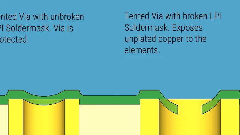
A tented via with unbroken solder mask protects the via vs. a tented via with broken LPI soldermask that exposes unplated copper to the elements
This article was first published on
macrofab.comVia Tenting for PCB Design
Tenting a via refers to covering via with solder mask to enclose or skin over the opening. A via is a hole drilled into the PCB that allows multiple layers on the PCB to be connected to each other. A non-tented via is just a via that is not covered with the solder mask layer. Leaving these vias exposed or covered has pros and cons depending on your design and manufacturing requirements.
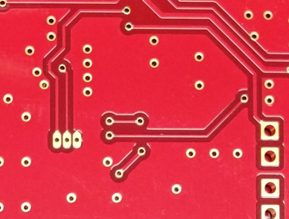
Exposed vias on a ground plane and signal paths.
LPI solder mask covered vias to create tented vias.
Soldermask Basics
The solder mask that MacroFab and most pcb fabrication houses use is called an LPI (Liquid PhotoImageable) solder mask. LPI solder mask is usually a two-part mixture that is UV curable. It is applied with a screen printing process onto the PCB and then UV-cured to a hard finish. Soldermask provides a physical barrier to prevent damage to the PCB copper layers and has a high electrical isolation rating of around 2.5 × 10¹² Ω.
Why Would You Want to Cover a Via with Soldermask?
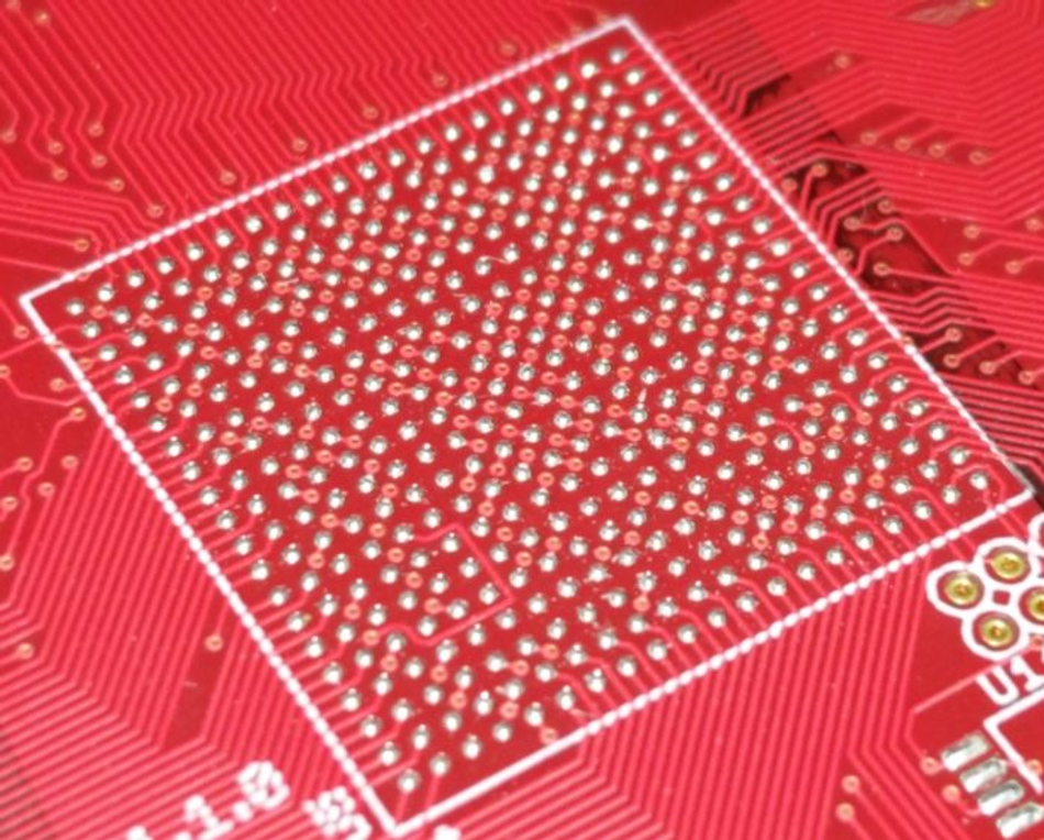
The role of the PCB’s solder mask is to protect the copper traces from damage, oxidation, and solder bridging. These protections also apply to the vias. Tented vias will be more resistant to physical damage and electrical shorts. If your PCB design has through-hole components that will be wave soldered then a tented via will prevent the solder from flowing up into the via and over the other side of the PCB where it can potentially short out components. Vias that are also in close proximity to SMT pads should also be tented. This will prevent the solder paste from wicking into the via and creating a poor solder joint. This is especially important with dogbone-style BGA escaping.
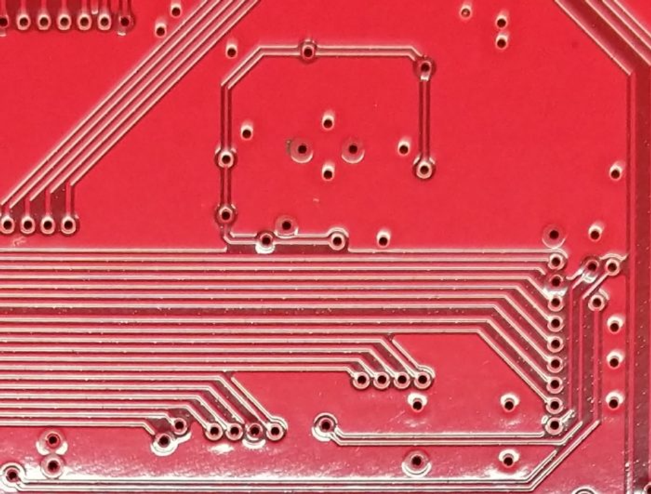
BGA breakout using via dogbone style routing. Vias are tented to prevent solder paste from flowing into the via.
Reasons for Exposing a Via
Tenting vias does have its downsides. Since the LPI solder mask is a liquid, it has to “bridge” the gap over the via hole. This can cause the solder mask to not completely tent the via leaving a small hole. The small hole can provide a way for corrosive flux, moisture, and other chemicals to enter the via being trapped. This can enable the possibility of a failure of the via due to corrosion eating the copper via. This is less of an issue due to the popularity of no clean flux for SMT assembly but corrosive water clean flux is still prevalent in through-hole assembly.
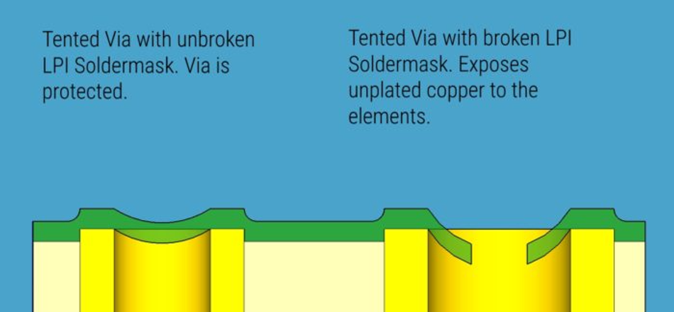
Small via on the left with an unbroken LPI Soldermask which protects the via. The larger via on the right has a broken via tent. This is due to the LPI solder mask’s liquid nature and trying to cover too much of a span.
Leaving the vias exposed without solder mask does not mean the copper will be open to the environment. The exposed vias will be plated by the surface finish of the PCB. At MacroFab we use the ENIG finish which will cover the insides of exposed vias with gold, protecting the copper from corrosion and damage.
For projects that are still in the prototyping phase, it can be beneficial to have the vias exposed to be able to fix and reroute traces and be used as impromptu test points.
Using the MacroFab Platform to Check Via Coverage
The PCB interface on the MacroFab platform provides an easy way to check the vias in your design to see if they are tented or not. Simply upload your design files and check the PCB render. Tented vias will show as just the drill holes with solder mask covering the copper. Exposed vias will have the solder mask pushed back from the annular ring for the via showing the ENIG finish in the PCB render.
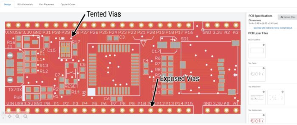
How tented vias and exposed vias look in the MacroFab PCB Platform.
Recap
So should you tent your vias, or not? For long-term reliability of the PCB, and improved manufacturability of the PCB, it is better to seal the via completely to prevent ingress of moisture and fluids. Doing this economically can be a problem. Filling vias with epoxy and capping (to be explained in a future article!) can be costly. Whether or not tenting a via with LPI solder mask can be done reliably depends on the size of the via. The smaller the via, the easier it is for the via to be filled. After a certain point, the vias are too large and tenting can not be done. This tends to be around 15mil diameter for the via with the LPI solder mask used by MacroFab’s PCB manufacture. Vias larger than 15mils should be left exposed so they can be plated with ENIG surface finish instead of relying on the LPI solder mask to seal the via. These larger vias should be kept away from areas with solder paste to prevent paste from wicking away from the pad area. Make sure vias under BGA parts, or vias right next to SMD pads, are tented. When I design boards, I generally leave vias of any size exposed unless they are right next to an SMD pad.