Understanding the SR Latch: Theory, Design, Truth Tables and Practical Implementations
This article explores the basics of SR Latch, covering its fundamental principles and implementation using NOR and NAND gates, metastability and race conditions, illustration of gated variants and real world applications such as switch debouncing and integrated latch ICs.

05 Dec, 2025. 14 minutes read
SR Latch, Truth Table
Key Takeaways
SR Latches Store a Single Bit – By cross‑coupling two logic gates, the latch maintains its state until explicitly set or reset.
NOR and NAND‑based Implementations Differ – NOR latches are active‑high while NAND latches are active‑low; both have an illegal input combination that must be avoided.
Metastability and Race Conditions Matter – Asserting both set and reset simultaneously can produce an undefined state due to critical races, which designers must avoid.
Gated SR Latches Introduce an Enable Input – Adding an enable signal controls when the latch is responsive and prevents unwanted changes.
Practical Applications – SR latches are used for switch debouncing, as simple memory elements, for control logic, and as building blocks for more complex latches and flip‑flops.
Introduction
The SR latch is one of the most fundamental building blocks in digital electronics, forming the basis of memory and state-holding circuits. Its primary function is to store a single bit of information, while also ensuring system stability and controlling sequential logic behavior. The "SR" stands for Set and Reset, the two primary inputs. This essential component is crucial for understanding more complex memory elements, such as flip-flops. Designing the basic SR latch involves cross-coupling two logic gates, typically NOR or NAND gates. The resulting structure creates a feedback loop that maintains its output state.
This article delves into the theory behind the SR latch, explores implementations using NOR and NAND gates, and examines gated SR latches that incorporate enable control. It also discusses metastability, race conditions and the undefined state that occurs when both set and reset inputs are asserted simultaneously. Throughout, real‑world examples illustrate how SR latches are used in debouncing circuits and as building blocks for larger memory systems.
Fundamentals of Bistable Circuits
Memory in Digital Logic
Digital systems need memory elements to store intermediate results, configuration bits, and state information. Unlike combinational circuits, which respond only to current inputs, sequential circuits use storage elements to hold data across clock cycles. Latches and flip‑flops are the fundamental storage elements; each can store one bit. The difference between latches and flip‑flops is that latches respond to their inputs whenever an enable signal is asserted (level‑sensitive). In contrast, flip‑flops capture input values only on specific clock edges (edge‑triggered).
The simplest storage element is a bistable element made by connecting two inverters in a loop. Because the outputs feed back into the inputs, the circuit has two stable states — logical high or logical low — and it remembers which state it was in when power was applied. However, since there are no inputs, the stored bit cannot be changed without interrupting power. Introducing inputs to control the state leads to the SR latch.
Positive Feedback and Hysteresis
The feedback mechanism in a latch provides positive feedback — the output reinforces the input so that once the latch is set or reset, it stays in that state. Positive feedback creates hysteresis, meaning a small change at the input does not immediately change the output; the latch “remembers” its previous state.
For example, a set command drives one output high and the other low. Once the set command is removed, the high production continues to feed back into the other gate, keeping the latch set. Similarly, a reset command drives the output low, and the latch remains reset even when the input returns to its inactive state.
This self-reinforcing behavior prevents oscillating outputs and forms the foundation of predictable sequential logic. When combined with structured inputs, controlled timing, or additional gating, positive feedback becomes the core mechanism enabling practical devices such as the gated SR latch, D latch, SR flip-flop, and more advanced elements like the JK flip-flop.
Recommended Reading: Understanding Transistors: What They Are and How They Work?
The SR Latch Constructed from NOR Gates
Circuit Description
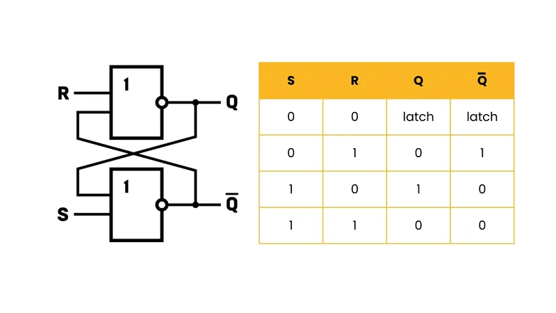
The SR latch is a fundamental memory element built from two cross-coupled logic gates, most commonly NOR gates. This configuration creates a bistable logic circuit, meaning it can hold one bit of data in either of two stable states. In a NOR-based SR latch circuit, one NOR gate receives the Set (S) input and generates the primary output Q, while the second gate receives the Reset (R) input and generates the complementary output Q̅. The outputs are tied back to each gate’s unused input, forming a feedback loop that maintains the stored state. [1]
When the set input S goes high, the upper NOR gate drives output Q high. This high level propagates to the lower gate, forcing Q̅ low, which in turn feeds back to keep Q latched. When the reset input R goes high, the opposite transition occurs: Q̅ becomes high, and Q goes low. When both S and R are low, the latch simply holds its previous state, making this configuration ideal for digital circuits, sequential logic, and basic data storage.
Truth Table and Behavior
The truth table below summarizes the behavior of the NOR‑based SR latch:
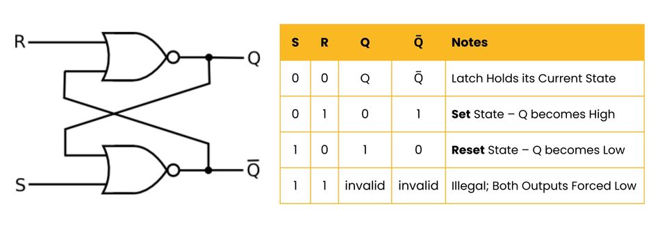
The illegal case (S = R = 1) violates the intended operation of the latch. Because both NOR gates force their outputs low, any eventual settling depends on minor manufacturing variations or input timing differences. This makes the resulting state unpredictable and must be strictly avoided in digital electronics and integrated circuits.
Metastability and Race Conditions
Despite its simple structure, the SR latch can exhibit complex timing behavior. When the set and reset inputs change nearly simultaneously, the cross-coupled gates may enter a metastable or oscillatory state. In this condition, neither output resolves immediately because each gate reacts to the other’s change — a phenomenon known as a critical race.
During a race condition, the latch momentarily hesitates between both possible stable states, and settling depends on minute variations in transistor delay, supply noise, or temperature. In extreme cases, the latch may remain metastable long enough to propagate erroneous levels to downstream sequential circuits.
Practically, designers prevent this by ensuring that S and R are never asserted together and never de-asserted simultaneously. Well-designed systems shape their input values, constraints, and control timing to eliminate this undefined region, keeping the SR latch reliable within larger digital logic structures such as flip-flops, shift registers, and synchronous systems.
Recommended Reading: Clock Gating: Powering Down Idle Circuits
The SR Latch Constructed from NAND Gates
Active-Low Inputs and Circuit Operation
The second common implementation of the SR latch uses two cross-coupled NAND gates instead of NOR gates. Despite the logic circuit structure being similar, the crucial difference is that the inputs are active-low, typically labeled S′ (active-low Set) and R′ (active-low Reset). In this arrangement, driving an input low asserts the corresponding function, while driving it high de-asserts it. [2]
Because a NAND gate outputs a logic-low only when both of its inputs are high, forcing S′ = 0 immediately drives output Q high. This occurs because “0 NAND x” always yields 1, establishing the set-reset state. When S′ and R′ both return to 1, the feedback loop preserves the stored bit, allowing the latch to maintain its previous state. This behavior makes the NAND-based SR latch circuit functionally equivalent to the NOR version, but with inverted input logic.
Active-Low Truth Table and Illegal Condition
Because of the inverted inputs, the truth table for the NAND implementation differs from the NOR-based latch:
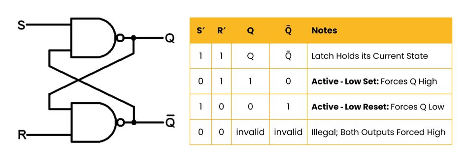
In particular, S′ = R′ = 0 is illegal because both outputs would be forced high, leading to the same metastability issues seen with the NOR version. The NAND implementation is often preferred in TTL logic because NAND gates are more common and are considered “universal” gates. However, designers must remember that 0 on an input asserts the corresponding function, whereas 1 de‑asserts it.
Timing Parameters and Propagation Delays
When building SR latches from discrete NAND or NOR gates, real hardware behavior depends heavily on timing parameters, propagation delays, and parasitic device characteristics. The typical propagation delay is 7 ns for the 74HC00 and 10 ns for the 74HCT00, as specified in their respective datasheets for a 5 V supply. [3] This delay defines how quickly the latch can safely change states and determines the maximum operating frequency of the digital logic system.
The additional timing parameters also influence performance! The datasheet further specifies an approximate input capacitance of 3.5 pF and a power-dissipation capacitance of about 22 pF per NAND gate. These capacitances — combined with any external resistors, capacitors, wiring length, and loading — affect rise/fall times, drive requirements, and susceptibility to noise.
In higher-speed sequential circuits, designers must ensure that the clock signal, enable paths, and input values allow sufficient settling time for the latch. Failure to account for propagation delay can lead to oscillating, undefined outputs, or metastable behavior.
Recommended Reading: Transistor as a Switch: Theory and Practical Implementation for Digital and Hardware Engineers
Gated SR Latches
Motivation for Gating
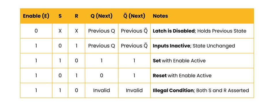
In practical digital logic systems, it is often necessary to prevent a basic SR latch from responding to its inputs until a specific control condition is satisfied. For example, a memory element may need to store a single bit only when new data is valid, or a control unit may want to update state exclusively during a defined phase of a clock signal. Introducing an enable input (E) transforms the circuit into a gated SR latch, allowing controlled data entry.
When E = 0, the input-gating logic gates drive both internal set and reset lines to 0, regardless of the external S and R signals. In this mode, the latch ignores changes to its inputs and maintains its previous state. When E = 1, the gating network becomes transparent, allowing S and R to influence the stored bit of data and update the stable states of the latch. This gating mechanism ensures predictable timing, reduces unwanted transitions, and prevents asynchronous changes from propagating deeper into sequential circuits.
Implementation
The gated SR latch can be built by preceding the ordinary SR latch with a pair of AND or NAND gates that combine the set and reset inputs with the enable signal. These gates combine the set-reset inputs with the enable signal:
E = 0, the AND-gate outputs become 0, effectively disabling the latch
E = 1, the AND gates forward the actual S and R input values to the storage element
This approach guarantees that the latch responds only during the enabled window. The resulting behavior is summarized in the truth table:
This gating mechanism is often used to synchronize latches with a clock or strobe signal. When the enable signal is driven from a clock, the circuit becomes an SR flip‑flop (edge‑triggered), which is more commonly used in synchronous digital designs. By controlling the enable, designers can ensure that latches change state only at appropriate times, avoiding glitches and race conditions.
Clocking and Synchronous Operation
The gating mechanism is widely used to synchronize latches with a clock input or strobe. When the enable pin is driven by a periodic clock, the gated structure effectively becomes the foundation of an SR flip-flop, which is an edge-triggered version suited for synchronous digital circuits. By ensuring that S and R propagate only during specific clock phases, designers eliminate glitches, timing hazards, and unintended state changes.
This transition from a simple latch to a clocked element forms the basis of more advanced storage devices such as the D latch, JK flip-flop, and the many flip-flop types used in shift registers, counters, and modern integrated circuits. Controlled enabling is therefore essential for reliable, predictable, and noise-resistant sequential logic behavior.
Beyond SR Latches: D and Other Variants
D Latch — Eliminating the Illegal State
The key limitation of the basic SR latch is its potential illegal condition when both set and reset inputs are asserted simultaneously. This combination drives the latch into an unstable state, creating ambiguity and possible race conditions. The D latch addresses this weakness by ensuring that the two internal control signals can never be active at the same time.
Structurally, the D latch is simply a gated SR latch in which the S and R inputs are derived from a single data input (D). The internal inverter produces the complementary signal, so the latch receives S = D, R = D̅.
This arrangement guarantees mutual exclusivity — S and R cannot both be 1 — removing the illegal combination entirely. When the enable input is high, the D value propagates through the gating logic gates, forcing the output Q to reflect the new data. When enable is low, the latch preserves its previous state, making the D latch ideal for buffering and controlled data storage in digital circuits. Because it reliably stores a single bit without forbidden input patterns, the D latch is widely used in timing paths, sequential logic, and pipeline stages.
JK and T Latches
Although the SR and D latch families are the most commonly used bistable storage elements, additional latch structures extend their capabilities for specialized applications.
JK latch is a more flexible variant of the SR design. It allows both inputs (J and K) to be high simultaneously. Rather than entering an illegal state, the circuit toggles the stored bit when J = K = 1 and the enable is active. This eliminates the undefined region while providing a richer functional behavior. In edge-triggered form, the JK latch becomes the JK flip-flop, a classic building block used in counters, frequency scaling circuits, and programmable dividers.
The T latch simplifies this further. With only one toggle input (T), the output flips its value whenever T is asserted during the active portion of the enable or clock. When T = 0, the latch simply holds its state. In synchronous form, the T flip-flop is widely used in binary counters and ripple-divider chains because each toggle represents a predictable half-frequency transition.
Understanding the operation of the SR latch — its stable states, its feedback mechanisms, and its input constraints — forms the conceptual foundation for these more advanced latch and flip-flop architectures.
Practical Implementations
Building an SR Latch with Discrete Gates
Experimenters can build an SR latch using discrete NOR or NAND gates. The CD4001 CMOS chip contains four NOR gates; connecting two of them in a cross‑coupled configuration yields a functional SR latch. The 74HC00 or 74LS00 chips provide four NAND gates that can be used to build the active‑low version. When constructing the circuit on a breadboard, pay attention to power supply connections, unused inputs, and proper feedback wiring.
The typical implementation uses 2 push buttons and 2 LEDs. Pressing the Set button asserts S (or drives S′ low), illuminating one LED. Pressing Reset asserts R and lights the other LED. Because of its bistable structure, the latch maintains its previous state even after the buttons are released.
Integrated SR Latch ICs
For higher reliability and predictable timing, designers often use dedicated integrated circuits that implement multiple SR latches in a single package. Devices such as the 74LS279 and 74HC279 contain four independent latches with active-low reset inputs and well-defined propagation delays, fan-out, and power characteristics. These parameters simplify timing analysis in larger digital circuits and help avoid race conditions.
Beyond standalone chips, many microcontrollers, FPGAs, and ASICs internally implement latch-based storage. For example, SRAM cells consist of two cross-coupled inverters — a direct descendant of the classic SR latch. Understanding how the latch works at the transistor level clarifies the behavior of these dense memory structures, especially regarding stability, noise margin, and data storage reliability.
Debouncing Mechanical Switches
Mechanical switches inherently suffer from contact bounce, producing rapid on-off transitions before settling. If such a switch drives a counter, interrupt line, or synchronous input, these transitions may generate multiple unintended triggers.
A traditional hardware solution inserts a cross-coupled NAND-gate SR latch between the switch and downstream logic. The UNC Charlotte laboratory manual describes a debouncing circuit using a double-pole single-throw (DPST) switch that keeps both S′ and R′ high during idle conditions. [4] Once the switch toggles, one input momentarily drops low, setting or resetting the latch.
Because the latch transitions only when one input value is low and the other is high, contact bounce simply forces the latch to alternate between the asserted state and the latched state — without producing additional output transitions. This yields a single, clean edge at the latch output and is widely used in embedded systems where reliable switch behavior is essential.
Timing and Noise Considerations
When designing SR latches, engineers must consider timing and noise. Real gates have non‑zero propagation delay, and differences between the delays of the two gates can determine how quickly the latch settles. Propagation delay also sets the maximum frequency at which a latch can operate. Devices with Schottky or CMOS technology often offer faster switching times but may require careful termination to prevent ringing. Additionally, SR latches have setup and hold time requirements when used in synchronous designs; violating these can cause metastability.
The noise margin is another critical parameter! Because latches rely on positive feedback, small noise spikes at the inputs can inadvertently switch the latch. Using hysteresis (e.g., Schmitt triggers) or gating the latch with an enable signal helps reduce susceptibility to noise. In integrated circuits, designers often implement cross‑coupled transistors with carefully matched geometries to maximize noise immunity.
Recommended Reading: Types of Switches: Complete Engineering Guide for 2025
Applications of SR latches
Memory and Storage Elements
The SR latch acts as a single-bit memory element capable of holding a previous state indefinitely through positive feedback. In more complex systems, arrays of latches form registers and register files. For example, an 8‑bit register can be built from eight SR latches (usually as part of a D latch or flip‑flop) that share a common enable line. In FPGAs, configuration bits are often stored in a lookup table (LUT) memory, which uses SRAM cells built from cross‑coupled inverters.
State Machines and Control Logic
Simple state machines can use SR latches to remember whether a particular condition has been met. For instance, a hardware controller may need to record that a sensor threshold has been exceeded and remain in that state until a reset signal arrives. Cross‑coupled latches also appear in asynchronous control circuits, such as priority encoders or arbitration circuits, where the order of events must be remembered.
Edge Detection and Pulse Stretching
SR latches combine naturally with logic gates to implement edge detectors and pulse-conditioning circuits. By applying a narrow input pulse to the set input and then issuing a delayed reset, the latch produces a pulse of controlled width regardless of the original pulse duration. This is useful when working with sensors, oscillators, or digital interfaces that produce pulses too short for downstream circuits to detect. Such circuits are widely used in timers, counters, microcontroller interrupt inputs, and synchronization units.
Debouncing and Noise Filtering
One of the most common uses of SR latches is switch debouncing. By eliminating spurious transitions caused by mechanical bounce, the latch ensures that control signals change state only once per switch action. This prevents unintended multiple triggers, especially when interfacing with counters, flip-flops, or interrupt-driven microcontrollers. Engineers also employ latches as noise filters, which reject short glitches that might otherwise propagate through combinational logic.
Recommended Reading: What is an Encoder: Understanding the Basics and Beyond
Design Considerations and Pitfalls
Avoiding the Illegal State
The most important rule when using SR latches is never to assert both set and reset inputs simultaneously. Doing so can cause the latch to enter a metastable state, where its outputs become unpredictable. In synchronous designs, the gating logic should ensure that only valid input combinations reach the latch. Designers often add logic to detect and prevent illegal states or incorporate latches that inherently eliminate them, such as the D latch or JK latch.
Dealing with Metastability
Even when inputs are valid, small timing differences between gates can push the latch into metastability. To mitigate this, latches used in asynchronous inputs (e.g., crossing clock domains) should be followed by synchronizer circuits — usually two or more flip‑flops in series — to allow metastable states to resolve before signals are used by downstream logic. Properly designing input filters and using Schmitt triggers can also reduce the likelihood of metastability.
Level-Sensitive vs. Edge-Triggered Storage
Latches are level‑sensitive, meaning they respond to inputs whenever the enable is asserted. In contrast, flip‑flops capture inputs only on clock edges and are immune to glitches occurring between edges. When designing a synchronous system, flip‑flops are usually preferred because they simplify timing analysis. However, latches offer advantages in power and area, and modern high‑performance designs sometimes use two‑phase latch pipelines to reduce clock skew and increase throughput. Understanding SR latches helps designers appreciate these trade‑offs.
Conclusion
The SR latch remains the foundational building block of digital logic, demonstrating how simple cross-coupled gates can store a single bit and maintain a stable system state. NOR-based latches use active-high control, while NAND-based versions use active-low inputs, yet both provide essential set, reset, and hold behavior. Designers must avoid illegal input combinations to prevent metastability and ensure reliable operation. Introducing an enable signal creates the gated SR latch, enabling controlled state transitions in larger systems. Mastering SR latches builds intuition for more advanced structures such as D latches, flip-flops, counters, and memory arrays, and provides practical insight for debouncing, pulse conditioning, control logic, and hardware design.
Frequently Asked Questions (FAQs)
1. What is the difference between an SR latch and a flip-flop?
A. SR latch is a level-sensitive set-reset latch, while a flip-flop is edge-triggered and isolates glitches more effectively. Flip-flops suit synchronous systems, whereas latches remain useful in low-power or asynchronous designs.
2. Why is the S = R = 1 condition illegal in an SR latch?
A. This input combination breaks Q/Q̅ complementarity in the circuit diagram, driving both outputs to the same value. The resulting critical race can push the latch into an undefined state.
3. How does a gated SR latch differ from a basic SR latch?
A. A gated latch adds an enable line that blocks inputs when inactive. It lets designers control state updates with a clock, strobe, or even a multiplexer-driven enable path.
4. How can I implement a simple switch debouncer with an SR latch?
A. NAND-based set-reset latch paired with a DPST switch removes bounce-induced glitches. Many engineers follow a debouncing tutorial that uses pull-ups, clean wiring, and predictable feedback behavior.
5. When should I use a D latch instead of an SR latch?
A. Use a D latch when you must prevent illegal set-reset combinations. Its internal inverter ensures safe complementary inputs without external diodes or extra gating.
6. What are typical propagation delays for SR latches?
A. Delays depend on the logic family, with CMOS NAND or NOR gates typically around 7–10 ns. Always verify timing in the component datasheet before finalizing a high-speed design.
References
[1] Educative. The SR latch [Cited 2025 November 10] Available at: Link
[2] ResearchGate. SR Latch: The Wrong Introduction to Digital Memory [Cited 2025 November 10] Available at: Link
[3] UTEXAS. 74HC00; 74HCT00 Quad 2-Input NAND Gate [Cited 2025 November 10] Available at: Link
[4] UNC Charlotte. Laboratory Manual - Switch Debouncing [Cited 2025 November 10] Available at: Link
in this article
1. Key Takeaways2. Introduction3. Fundamentals of Bistable Circuits4. The SR Latch Constructed from NOR Gates5. The SR Latch Constructed from NAND Gates6. Gated SR Latches7. Beyond SR Latches: D and Other Variants8. Practical Implementations9. Applications of SR latches10. Design Considerations and Pitfalls11. Conclusion12. Frequently Asked Questions (FAQs)13. References