What Is Ground in a Circuit? Understanding Grounding Concepts and Implementations
Ground is the reference point that makes voltage meaningful and the return path that allows current to flow. This article explains what is ground in a circuit, discusses different types of grounds, and shows how to implement effective grounding strategies

19 Nov, 2025. 13 minutes read

Key Takeaways
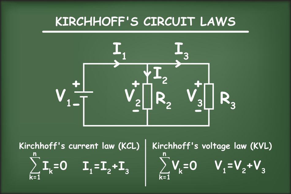
Ground is a reference and a return path. The voltage is always measured between two points, so a common reference point (ground) defines 0 V and allows consistent measurements. At the same time, ground provides the current return path required by Kirchhoff’s laws.
Different types of ground serve different roles. Earth (safety) ground protects against electric shock, chassis ground connects enclosures to a safe potential, and signal ground establishes a 0 V reference for circuit operation. Mixed‑signal systems often separate analog and digital grounds to reduce noise.
Grounding affects noise and signal integrity. Changing currents in ground return paths create voltage variations and noise. Improper ground layouts (ground loops or split planes) cause EMI and degrade sensitive signals.
PCB grounding strategies are critical. Single‑point grounding suits low‑frequency circuits, while multi‑point grounding and ground planes support high‑speed designs. Star or partitioned grounds help isolate analog and digital sections.
Ground is not always zero volts. Since real conductors have resistance, large ground regions develop potential differences (ground offsets) and may not be exactly at 0 V.
Introduction
Ground is one of the more familiar symbols for every electrical engineer. It’s a series of horizontal lines that disappear into a page. Yet what is ground in a circuit?
In theory, ground is the point of zero potential.
In practice, ground is the common reference node used to measure voltages and the path that currents take when returning to their source.
Unless a circuit has a well-defined ground, voltage measurements are meaningless, and current has no return path to complete the circuit. Hence, ground plays a dual role as reference and return. However, its implementation depends on the application, whether it is a battery‑powered sensor, a mains‑connected appliance, or a high‑speed mixed‑signal PCB.
For designers and engineers, understanding ground is critical because improper grounding can cripple performance. Mixed‑signal boards require careful partitioning of analog and digital grounds, ground loops can inject hum into audio systems, and high‑frequency circuits depend on ground planes for signal integrity. As data rates increase and devices shrink, the seemingly mundane concept of ground becomes a design challenge.
Suggested Reading: Open Circuit vs Short Circuit: Core Differences between Open and Closed Circuit
What Ground Means in Circuit Theory
Reference Point and Relative Measurement
While analyzing circuits, voltage is always treated as a relative quantity. It means that it is always measured between two nodes. So, there must be a reference node with a potential defined to 0V, simplifying measurements and calculations. This reference node is called ground or GND.
All other voltages in the circuit are measured with respect to this node. So, a voltage of 5 V means that the potential difference between a node and ground is five volts. Ground thus establishes a common baseline for measurements across the entire system.
Return Path
In addition to being a reference point, a ground node is also the point where current returns to the source. For a circuit to function, current must flow in a closed loop. Regardless of how complex a design becomes, there is always a trace or plane that serves as the return path for current to get back to its source.
In many circuits, these return paths are collectively called “ground”. Recognizing ground as the return path is essential in PCB layout and high‑frequency design.
Ground vs. Negative Supply
In most circuits, the negative terminal of the power source is treated as ground. However, it’s not a fixed rule. In single‑supply systems, the negative terminal is usually chosen as ground because it is convenient to define 0 V there.
But practically, ground can be any node in the circuit. In split‑supply systems (±12 V or ±5 V), ground lies between the positive and negative rails. The negative rail is then at –V with respect to ground.
Thus, ground is defined by convention, not by hardware. Some circuits even operate without a connection to earth or chassis; the reference node floats with respect to earth but still functions as ground.
Ideal and Real Ground
Textbook circuit theory treats ground as an ideal node that can absorb or supply unlimited charge with zero resistance. But in reality, all conductors have finite resistance and inductance. Large ground regions, such as copper planes on a PCB, exhibit potential differences across their length. Due to this resistance, conductors at different points on a ground plane are not always at exactly 0 V; instead, there may be a ground offset due to voltage drops across the return path.
High‑frequency currents produce voltage variations in ground return paths, and these variations can couple into sensitive signals. Engineers often speak of a “noisy ground” when return currents cause voltage fluctuations.
The non‑ideal nature of ground is important for high‑accuracy systems. Systems such as mixed‑signal devices, analog‑to‑digital converters (ADCs), and digital‑to‑analog converters (DACs) require stable reference grounds. Therefore, proper layout and grounding strategies aim to minimize impedance and keep ground potential differences small.
Suggested Reading: How to Design a PCB Layout: A Comprehensive Guide
Functions of Ground
Ground performs several key functions in electronic systems:
Voltage reference — Ground provides a reference point to measure voltages. All voltages are defined in terms of the electric field between two points; one of these points is defined as 0 V, often called a reference plane.
Return path — Ground completes the circuit by providing a path for current to return to the power source. Without a return path, current cannot flow.
Charge reservoir and field terminator — Ground acts as a large reservoir of charge that defines the direction of current flow. It also provides a point where electric fields terminate; in electromagnetics problems, ground is an equipotential surface at 0 V.
Shielding and EMI control — A properly designed ground plane shields sensitive circuits by terminating stray electric fields and providing a low‑impedance path for high‑frequency currents.
Safety — Earth ground protects users from electric shock by providing a low‑impedance path for fault currents to trip breakers. Chassis ground connects equipment enclosures to a safe potential.
Types of Ground
Grounds have different purposes in various systems. Among the common types of ground are:
Earth ground
Chassis ground
Signal (common) ground,
Analog/digital ground.
Based on the system and requirements, engineers and designers may pick the appropriate type. Here is a table that illustrates the purpose and implementation:
Type of ground | Purpose | Typical implementation |
Earth ground | Provides a low‑impedance path to the Earth to prevent electric shock. | Metal rod driven into Earth; connected to building wiring |
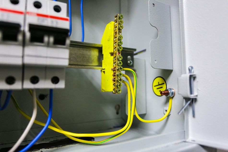
Chassis ground | Connects the metallic enclosure of a device to earth or a reference point | Enclosure connected via green wire to the safety ground. |
Signal or common ground | Serves as the 0 V reference node for voltage measurements. | Copper plane or trace on PCB |
Analog ground | Reference for analog circuitry | Dedicated plane or region on PCB |
Digital ground | Carries noisy return currents from switching logic | Plane or region labelled DGND |
Safety or protective earth (PE) | Conducts fault currents away from exposed metal parts | Third prong in AC plugs |
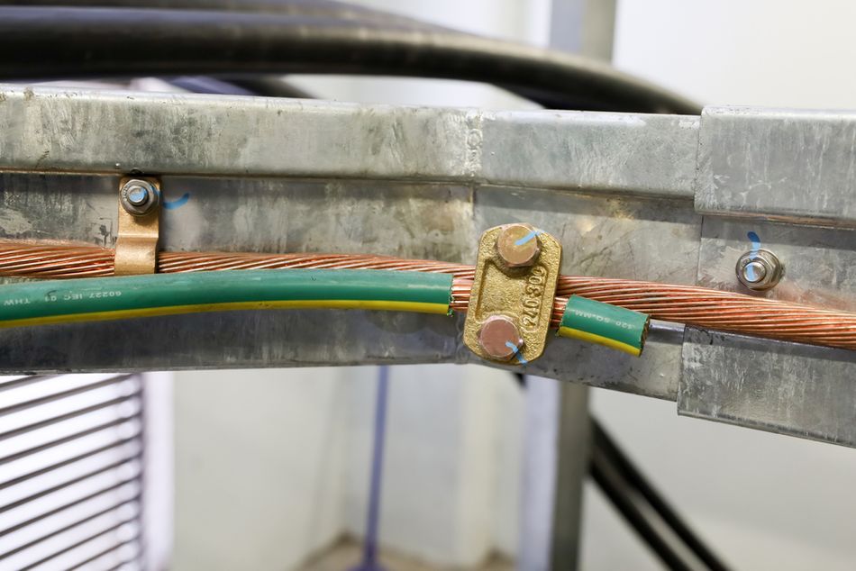
Earth Ground
It is the physical connection to the soil. Power distribution systems drive a metal rod or pipe into the earth to create a neutral reference. The earth offers a virtually infinite reservoir of charges, so its potential does not change appreciably when current flows.
Earth ground is not intended to carry operational currents; it dissipates fault currents, lightning strikes, and static electricity.

Chassis Ground
Chassis ground uses the metal enclosure of a device as a reference. Connecting the chassis to earth ground shields the internal circuitry and protects users. The chassis acts as a Faraday cage and provides broadband shielding, dissipating spurious currents and electromagnetic interference.
Chassis ground is often connected to the protective earth in three‑wire systems (hot, neutral, and ground). In battery‑powered or plastic‑enclosed devices, there may be no chassis ground.
Signal Ground
Signal ground is the node used as the reference for voltage measurements and as the return path for circuit currents. It’s usually known as ‘common’ in electrical and electronic circuits. It is usually implemented as a large copper plane or trace on the PCB to provide low impedance.
In most electrical designs, common ground is named as GND, 0V, or COM. It is also important to note that signal ground may be floating with respect to earth.
Suggested Reading: What is GND in a Circuit: The Complete Guide for Digital Design and Hardware Engineers
Analog and Digital Grounds
Analog ground (AGND) and digital ground (DGND) separate return currents in mixed‑signal systems.
Digital circuits generate large, fast current spikes when signals switch states.
Analog circuits process small signals and are sensitive to noise.
The segregation of grounds is important because if digital return currents flow through the analog ground, they induce voltage drops (noise) that corrupt analog measurements.
Therefore, designers often isolate AGND and DGND planes and join them at a single point (the star ground).
Functional and Virtual Grounds
Some circuits use functional grounds such as a virtual ground or a mid-supply reference. In an op‑amp circuit powered from a single supply, a resistor divider may create a mid‑rail reference at half the supply voltage. This node serves as a pseudo‑ground for AC signals.
Virtual ground circuits use active components to maintain a reference at a desired potential. These functional grounds do not connect to earth; they provide a convenient reference for specific circuit blocks.
Ground as a Current Return Path
Kirchhoff’s Laws and Closed Loops
Current flows in closed loops as described by Kirchhoff’s current law: the algebraic sum of currents entering and leaving a node is zero. For any circuit, there must be a path for the current to return to the source.
The return path often runs through the ground conductor or plane. If there is no return path, no current flows. For example, connecting a load between a positive terminal and the earth ground of a power supply may seem reasonable to beginners, but no current will flow because the return path to the supply is missing. The proper connection is between the positive and negative terminals of the supply.
Signal Return Paths in PCBs
On a PCB, every signal has a return current. At low frequencies, the return current takes the path of least resistance, typically the shortest route through the ground network. At high frequencies, return currents follow the path of least impedance, often directly beneath the signal trace in the adjacent ground plane due to inductive coupling.
When signals cross splits or cuts in the ground plane, the return current is forced to take a longer path, increasing loop area and generating electromagnetic radiation.
Suggested Reading: Trace Width vs Current in PCB Design
Grounding Strategies in PCB Design
Proper grounding in printed circuit boards ensures signal integrity, reduces electromagnetic emissions, and protects sensitive components. The choice of strategy depends on the circuit’s frequency content and complexity.
Single‑Point Grounding
Single‑point or star grounding ties all ground connections to a single point. This scheme minimizes ground loops because there is only one return path. It works best for low‑frequency circuits or small designs where signal speeds are below about 1 MHz. For example, audio amplifiers often use star grounding: all ground leads from the preamp, power amp, and input jacks converge at a single node near the power supply. This arrangement minimizes hum and prevents crosstalk among channels.
The star grounding philosophy appears simple, but can be difficult to implement in practice. Large systems require long conductors to reach the star point, which increases impedance and noise. When power supplies and high‑current paths are added, unwanted ground paths can form, corrupting the star point.
Multi‑Point Grounding
Multi‑point grounding attaches ground connections at multiple locations, typically through a ground plane. This approach is preferred for high‑frequency designs (above 10 MHz) because it shortens return paths and reduces impedance. Each signal can return to the nearest ground point, minimizing loop area.
Multi‑point grounding is also used in large digital systems with multiple boards or modules. However, designers must ensure that these multiple connections do not create unintended loops; all ground points should connect through a continuous low‑impedance path.
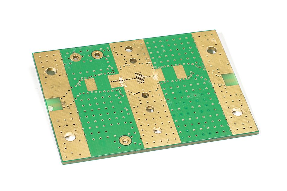
Ground Planes
A ground plane is a contiguous layer of copper dedicated to ground in a multilayer PCB. It provides a low‑impedance reference for all signals and a direct return path for currents.
Ground planes reduce noise and electromagnetic interference (EMI) by containing current loops and shielding adjacent layers. In a four‑layer board, one layer is often dedicated to ground; in high‑speed designs, the impedance of the ground plane can be below 0.01 Ω at high frequencies.
When using ground planes, avoid splitting them unnecessarily. Splits force return currents to detour around gaps, increasing loop area and radiation. If a split is necessary (e.g., to separate analog and digital grounds), provide a bridge or controlled connection so that signal traces cross only at that bridge.
Suggested Reading: What is a Multilayer PCB?
Ground Loops in PCB Layout
Ground loops are not confined to audio systems; they also occur in PCBs when there are multiple paths between two ground nodes. For instance, connecting the ground at both ends of a shielded cable and also through a ground plane creates a loop. High‑frequency switching currents can induce voltage differences, injecting noise into analog circuits. To mitigate loops:
Use single‑ended connections for shields—connect at the receiver end only.
Keep ground traces and planes short and wide to reduce impedance.
Consolidate ground connections to a common point on the board.
Grounding in Specific Applications
Digital Circuits and Logic Boards
Digital logic circuits generate fast rising and falling edges that draw high di/dt currents from the power supply. These currents return through ground and can cause ground bounce and simultaneous switching noise. Strategies for digital boards include:
Solid ground plane — A continuous ground layer provides a low‑inductance return path and reduces ground bounce.
Decoupling capacitors — Place capacitors close to power pins to supply transient current locally and relieve the ground plane.
Power and ground pins — On FPGAs or processors, connect multiple ground pins to minimize inductive drops. Use via stitching to connect power planes to ground.
Analog Circuits and Precision Measurements
Analog circuits, such as operational amplifier stages and low‑level sensors, require low‑noise ground references. Here are some key guidelines:
Dedicated analog ground — Use a separate region or plane for analog circuits; connect to digital ground at one point.
Kelvin connections — For current sensing or precision shunt resistors, route separate sense lines directly to the measurement device to avoid ground drops.
Guard rings — Surround high‑impedance nodes with guard traces connected to ground to reduce leakage and interference.
Isolated grounds — In instrumentation amplifiers or differential amplifiers, use differential measurement to reject ground noise.
Suggested Reading: Inverting vs Non Inverting Op Amp: Complete Design Guide & Best Practices 2025
High‑Speed Interfaces and RF
RF circuits and high‑speed serial interfaces (such as USB 3.x, PCIe, or LVDS) demand meticulous grounding because return currents follow the path of least impedance at high frequencies. Here are some recommendations for high-speed PCB grounding:
Coplanar or stripline — Implement controlled-impedance transmission lines with adjacent ground reference.
Via fences — Surround high‑speed traces with ground via fences to confine fields and reduce crosstalk.
Ground shielding — Use coax cables or twisted pairs with a ground reference for external connections.
Avoid ground stubs — Stubs and vias in ground planes create resonances; use back drilling or blind vias to reduce stub length.
Suggested Reading: Expert Tips for High-Speed Backplane PCB Design
Safety and EMC Considerations
In mains‑powered equipment, safety regulations require protective earth connections. The ground conductor must carry fault currents to trip breakers and prevent hazardous voltages on exposed parts. Never remove the ground prong to fix hum; use isolation transformers or hum eliminators instead.
For electromagnetic compatibility (EMC), chassis ground and shielding enclosures reduce radiated emissions and susceptibility. Connect the chassis ground to earth near the power entry point and tie the PCB ground to the chassis at a single location.
Suggested Reading: EMI Shielding: Protecting Electronic Devices in a Noisy World
Troubleshooting Ground Problems
Ground issues often manifest as hum, oscillation or erratic behaviour. A systematic approach helps identify and fix them.
Visual inspection — Check for broken ground traces, missing vias, and improper solder connections.
Measure ground potential differences — Use a multimeter to measure voltage differences across ground points. Unexpected voltage indicates a ground offset or a loop.
Check return path continuity — Ensure that the current has a clear path back to its source. Look for connections that bypass the negative supply terminal.
Isolate sections — Disconnect subsystems to see if noise originates from a particular section. Reconnect with proper star or partitioned grounding.
Use differential probes — For measuring high‑frequency signals, differential probes avoid referencing to a potentially noisy ground.
Simulate — Use circuit simulation tools to model return paths and identify potential ground loops or resonances.
Suggested Reading: Electrical Testing: Comprehensive Guide for Engineering Professionals
Conclusion
Ground is a critical element in electronic circuits. While often depicted as a simple symbol, ground embodies the reference point against which voltages are measured and the return path that completes electrical loops. Real grounds are imperfect; finite resistance and inductance introduce noise and offsets.
Proper grounding strategies, such as star grounding, continuous ground planes, partitioning, and careful return path design, enable reliable digital and analog performance. Engineers must pay attention to grounding just as they do to power distribution and signal routing. As circuits become faster and more complex, grounding will remain a foundational concept that determines the success of the design.
FAQs
1. Why is ground considered 0 V in circuits?
Ground is assigned 0 V by convention to provide a reference point for measuring voltages. Voltage is a relative quantity; what matters is the potential difference between two points. By defining one point as 0 V, engineers can express other voltages relative to it. The chosen ground node need not be physically at zero potential relative to earth; it simply serves as the reference for the circuit.
2. What is the difference between ground and the negative terminal of a power supply?
In many single‑supply systems, the negative terminal is used as ground because it is convenient. However, ground is simply the reference node chosen for voltage measurements. In dual‑supply systems, ground lies between the positive and negative rails. The negative terminal is at a negative potential relative to ground. Thus, ground and the negative supply are not always identical.
3. Should I split analog and digital grounds on my PCB?
For most mixed‑signal designs, it is better to partition the PCB into analog and digital regions on a single continuous ground plane rather than physically splitting the plane. Splits force return currents to take long paths and act as antennas. Join analog and digital grounds at the mixed‑signal device or at a carefully chosen star point.
4. What causes ground loops and how can I eliminate them?
Ground loops occur when two points intended to be at the same potential are connected by multiple ground paths, forming a loop. The loop picks up interference and induces a voltage difference. Avoid ground loops by referencing all signal circuits to a single point, minimizing multiple return paths, and using differential signaling or isolation transformers in audio systems.
5. Can I connect signal ground to earth ground?
In most cases, signal ground is not directly connected to earth. The chassis ground may connect to earth for safety, and the signal ground may connect to chassis at one point. Directly connecting signal ground to earth can create large current paths and increase the risk of shock or EMI. Battery‑powered or isolated systems often do not use earth ground at all.
6. Why do analog and digital grounds need to be joined at one point?
Analog and digital grounds carry different types of current. Digital return currents are noisy and can corrupt analog signals. By joining analog and digital grounds at a single point (star point), designers ensure that digital currents do not flow through analog ground regions. This connection also provides a common reference so that ADCs and DACs can interpret signals correctly.
7. What is a ground plane and why is it important?
A ground plane is a continuous layer of copper in a PCB dedicated to ground. It provides a low‑impedance reference for all signals and a direct return path for currents. Ground planes reduce noise and electromagnetic interference by confining current loops and shielding adjacent layers. They are essential in high‑speed and high‑density designs.
References
All About Circuits, "An Introduction to Ground," Available: https://www.allaboutcircuits.com/technical-articles/an-introduction-to-ground/.
ALLPCB, "Effective Grounding Strategies: A Beginner's Guide to Quieting Your PCB Layout," Available: https://www.allpcb.com/allelectrohub/effective-grounding-strategies-a-beginners-guide-to-quieting-your-pcb-layout.
Texas Instruments, "Grounding in Mixed-Signal Systems," SLYT512, Available: https://www.ti.com/lit/pdf/SLYT512.
Altium Resources, "Stay Grounded: Digital, Analog and Earth Ground PCB Layout," Available: https://resources.altium.com/p/stay-grounded-digital-analog-and-earth-ground-pcb-layout.
Wikipedia, "Ground loop (electricity)," Available:
Circuit Cellar, "Find and Eliminate Ground Loops," Available: https://circuitcellar.com/resources/ee-tips/find-and-eliminate-ground-loops.
Analog Devices, "Staying Well-Grounded," Analog Dialogue, Available: https://www.analog.com/en/resources/analog-dialogue/articles/staying-well-grounded.html.
MadPCB, "Ground," Available: https://madpcb.com/glossary/ground.