The Ultimate Guide to Wafer Dicing: Techniques, Challenges, and Innovations
Wafer dicing separates individual integrated circuits or chips from a semiconductor wafer without damaging their delicate structures and circuits. This process is crucial for the production of electronic devices and components used in various industries, and the demand for it has increased with the development of high-performance and smaller electronic devices. Different dicing techniques, such as blade dicing, laser dicing, and plasma dicing, have been developed, and new innovations continue to emerge to address the challenges of complex semiconductor devices.

17 May, 2023. 26 minutes read
Introduction to Wafer Dicing
Wafer dicing is a crucial step in the semiconductor manufacturing process that involves the precise separation of individual integrated circuits (ICs) or chips from a semiconductor wafer. This process is essential for the production of electronic devices and components used in various industries, including consumer electronics, automotive, aerospace, and medical devices. As technology continues to evolve, the demand for high-performance and smaller electronic devices has increased, making wafer dicing even more critical.
The importance of wafer dicing lies in its ability to separate individual chips from a wafer without damaging the delicate structures and circuits embedded within them. The success of wafer dicing is measured by the quality and yield of the separated chips, as well as the overall efficiency of the process. To achieve these goals, several dicing techniques have been developed, each with its unique advantages and disadvantages.
In this article, we explore the importance of wafer dicing in semiconductor manufacturing, the techniques used, and the emerging innovations that address the challenges of complex semiconductor devices.
1. What are Semiconductor Wafers?
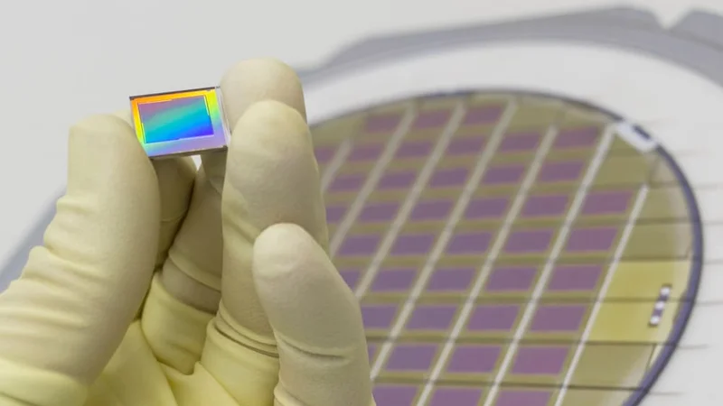
A semiconductor wafer is a thin, flat disc of semiconductor material, typically silicon, which serves as the substrate for the fabrication of integrated circuits (ICs) and other electronic devices. The wafer is the foundation upon which various layers of materials and patterns are built up to create individual electronic components and circuits.
Silicon is the most commonly used material for semiconductor wafers due to its excellent electronic properties, such as its ability to act as an effective insulator or conductor, depending on the addition of impurities. Silicon is also abundant, making it a cost-effective choice for the semiconductor industry. Other materials, such as germanium, Gallium Nitride (GaN), gallium arsenide (GaAs), and silicon carbide (SiC), are also used for specific applications, but they account for a much smaller share of the market compared to silicon.
1.1. The Process of Creating Semiconductor Wafer:
The process of creating a semiconductor wafer begins with the production of a large, single crystal of silicon, known as a boule. This is achieved through the Czochralski process or the float-zone method, both of which involve the controlled growth of a silicon crystal from a molten pool of high-purity silicon. Once the boule is produced, it is sliced into thin, flat wafers using a precision diamond saw. These wafers are then polished to achieve a mirror-like finish and ensure a smooth, defect-free surface for subsequent fabrication processes.
The diameter of semiconductor wafers has increased over time to accommodate the growing demand for more circuits per wafer, which improves manufacturing efficiency and reduces cost per chip. In the early days of semiconductor manufacturing, wafers were only 25 millimeters (mm) in diameter. Today, the industry standard for silicon wafers is 300 mm (12 inches), with some manufacturers even moving towards 450 mm (18 inches) wafers to further enhance productivity.
Semiconductor wafers undergo a series of complex fabrication steps, including photolithography, etching, and doping, which create intricate patterns of transistors, resistors, capacitors, and interconnects on the wafer surface. These patterns are formed on multiple layers, each serving a specific function in the electronic device. Once the fabrication process is complete, the wafer is subjected to wafer dicing to separate the individual chips, which are then packaged and tested before being integrated into electronic devices and systems.
2. Why Dicing is Important in Semiconductor Manufacturing?
Wafer dicing plays a significant role in maintaining the quality of the individual chips. As chips become smaller and more densely packed with electronic components, the risk of damage during the dicing process increases. This damage can manifest as chipping, cracking, or the deformation of the delicate structures within the chip, rendering it nonfunctional or prone to failure during operation. An effective wafer dicing process must minimize the risk of such damage while maintaining the structural integrity and performance of the separated chips.
One of the primary objectives of wafer dicing is to achieve a high yield of functional, undamaged chips from each wafer. The yield is a critical performance metric in semiconductor manufacturing, as it directly affects the cost and efficiency of producing electronic devices. A higher yield translates to a lower cost per chip and greater manufacturing capacity, enabling manufacturers to meet the increasing demand for electronic devices.
Wafer dicing has a direct impact on the overall performance of the electronic devices that incorporate the separated chips. The precision and accuracy of the dicing process ensure that each chip is separated according to the design specifications, with minimal variation in dimensions or alignment. This precision is essential for achieving optimal electrical performance, thermal management, and mechanical stability in the final device.
Recommended Reading: Wafer Probing: An Ultimate Guide
3. Common Wafer Dicing Techniques
There are several wafer dicing techniques employed in the semiconductor industry, each with its unique set of advantages and disadvantages. The choice of dicing technique depends on various factors, such as the material properties of the wafer, the size and density of the chips, and the desired quality and yield of the final product. In this section, we will explore the most common wafer dicing techniques: blade dicing, laser dicing, and plasma dicing.
3.1. Blade Dicing:
Blade dicing, also known as mechanical dicing, is the most widely used wafer dicing technique. It involves the use of a high-speed rotating blade coated with an abrasive material, typically diamond particles, to cut through the semiconductor wafer and separate the individual chips. The blade is mounted on a dicing saw, which accurately controls the position and depth of the cut to ensure precise separation of the chips according to the design specifications.
The primary advantage of blade dicing is its versatility and compatibility with a wide range of semiconductor materials, including silicon, germanium, and gallium arsenide. It is a well-established, cost-effective technique that can handle wafers of various sizes and thicknesses with relative ease.
However, blade dicing has some limitations, particularly when it comes to cutting smaller, more densely packed chips. As the blade cuts through the wafer, it generates mechanical stress, which can lead to chipping, cracking, or deformation of the delicate structures within the chip. Additionally, the width of the kerf (the material removed by the cutting process) can be quite large, resulting in a significant amount of material waste and a reduction in the number of chips that can be obtained from a single wafer.
To mitigate these issues, manufacturers have developed specialized dicing blades with ultra-thin profiles and advanced abrasive materials. These innovations help to reduce the mechanical stress and kerf width, minimizing the risk of damage to the chips and improving the overall yield and quality of the dicing process.
Another challenge associated with blade dicing is the need for an effective cooling mechanism. The friction generated by the cutting process can produce a significant amount of heat, which can cause thermal damage to the wafer and the chips. To counteract this, dicing saws are often equipped with a cooling system that uses a high-pressure jet of water or coolant to dissipate the heat and remove debris from the cutting area.
3.2. Laser Dicing:
Laser dicing or laser cutting is a non-contact wafer dicing technique that utilizes a focused laser beam to separate individual chips from the semiconductor wafer. The high-energy laser beam is directed at the wafer surface, inducing a process known as ablation or thermal decomposition, which vaporizes or removes the wafer material along the predetermined cut lines. There are several types of lasers used for wafer dicing, including ultraviolet (UV) lasers, infrared (IR) lasers, and femtosecond lasers. UV lasers are widely used for their high photon energy, which allows for precise, cold ablation with minimal heat-affected zones. This minimizes the risk of thermal damage to the wafer and the surrounding chips. IR lasers, on the other hand, are used for their deeper penetration into the material and are particularly suitable for thicker wafers. Femtosecond lasers generate extremely short pulses of light, enabling precise and efficient material removal with negligible heat transfer.
Laser dicing offers several advantages over traditional blade dicing. First, it is a non-contact method, which means there is no physical force applied to the wafer, reducing the risk of mechanical sawing, such as chipping and cracking. This makes laser dicing particularly suitable for the dicing of fragile or thin wafers, as well as wafers with densely packed or delicate features.
Another advantage of laser dicing is its high precision and accuracy. The laser beam can be focused down to a very small spot size, allowing for intricate cut patterns and the ability to separate chips with minimal spacing between them. This feature is particularly beneficial for advanced semiconductor devices, where the dimensions of the chips are continually shrinking.
However, laser dicing also has its limitations. The process can be slower and more expensive than blade dicing, particularly for high-volume production. Additionally, the choice of laser type and parameters must be carefully optimized to ensure efficient material removal and minimal heat-affected zones, which can be challenging for certain materials and thicknesses.
3.3. Plasma Dicing:
Plasma dicing, also known as plasma etching or dry etching, is another advanced wafer dicing technique that employs reactive ion etching (RIE) or deep reactive ion etching (DRIE) to separate individual chips from a semiconductor wafer. This technique uses a plasma, which is an ionized gas consisting of charged particles, to chemically remove material from the wafer along the predetermined cut lines. In the plasma dicing process, the semiconductor wafer is placed in a vacuum chamber, where a controlled mixture of reactive gases is introduced. An electric field is applied to the gas mixture, generating a plasma that contains a high concentration of reactive ions and radicals. These reactive species interact with the wafer material, selectively removing it along the cut lines through a combination of chemical reactions and physical sputtering. The etch rate and selectivity can be controlled by adjusting the plasma parameters, such as the gas composition, pressure, and power.
RIE and DRIE are the two primary plasma etching techniques used for wafer dicing. RIE is a more conventional plasma etching method, characterized by isotropic etching, where material is removed uniformly in all directions. DRIE, on the other hand, is an advanced etching technique that achieves highly anisotropic etching, enabling the formation of deep, vertical sidewalls with minimal lateral etching. This feature is particularly useful for the dicing of thick wafers and the fabrication of high-aspect-ratio structures.
One of the main advantages of plasma dicing is the reduction of mechanical stress on the wafer and chips. Since it is a non-contact method and does not involve any mechanical force, there is a lower risk of chipping, cracking, or deformation, which can be a concern with blade dicing. This makes plasma dicing especially suitable for fragile or stress-sensitive materials, as well as for wafers with advanced semiconductor devices that have complex or delicate structures.
Another advantage of plasma dicing is its high precision and accuracy. The etching process can be precisely controlled by adjusting the plasma parameters, allowing for intricate cut patterns and minimal spacing between chips. This feature is crucial for advanced semiconductor devices with shrinking dimensions, as well as for the dicing of non-silicon materials that have strict tolerance requirements.
The plasma dicing process can be complex and time-consuming, particularly for thick wafers or materials with high etch resistance. Additionally, the need for specialized equipment and gases can increase the overall cost of the dicing process, making it less attractive for high-volume production.
4. Factors to Consider When Choosing a Dicing Technique:
Selecting the most suitable wafer dicing technique is crucial for achieving the desired quality, yield, and cost-effectiveness in semiconductor manufacturing. Various factors must be considered when deciding which dicing method is best for a particular application. These factors include the material properties of the wafer, the size and geometry of the chips, the required precision and accuracy, and the overall production cost and efficiency.
4.1. Material Properties:
Different materials have varying levels of hardness, brittleness, and thermal sensitivity, which can impact the effectiveness of a dicing method. For example, blade dicing may be suitable for cutting silicon wafers, but it can cause chipping or cracking in more brittle materials such as gallium arsenide or glass. On the other hand, laser dicing and plasma dicing can be more suitable for fragile or stress-sensitive materials, as they are non-contact methods that minimize mechanical stress.
4.2. Chip Size and Geometry:
The dimensions and geometry of the individual chips on the wafer also influence the choice of dicing technique. For larger chips with simple geometries, blade dicing may be a suitable option due to its speed and cost-effectiveness. However, for smaller chips with intricate patterns or tight spacing, laser dicing or plasma dicing may be more appropriate, as these methods offer higher precision and can create narrower kerf widths.
4.3. Precision and Accuracy Requirements:
The required precision and accuracy of the dicing process depend on the specific application and device specifications. For advanced semiconductor devices with shrinking dimensions or strict tolerance requirements, high-precision methods such as laser dicing or plasma dicing are often preferred. These techniques enable intricate cut patterns and minimal chip spacing, ensuring that the final devices meet their performance and reliability specifications.
4.4. Production Cost and Efficiency:
The overall cost and efficiency of the dicing process are important factors to consider when selecting a dicing technique. Blade dicing, for instance, is generally faster and more cost-effective for high-volume production, as it requires less specialized equipment and consumables. However, the higher yield and lower material waste associated with laser or plasma dicing can offset the increased costs for certain applications, especially when dealing with expensive or scarce materials.
4.5. Environmental and Safety Considerations:
Lastly, environmental and safety considerations can also influence the choice of a dicing technique. For example, blade dicing can generate significant amounts of debris and slurry, which require proper disposal and can pose environmental and safety concerns. In contrast, laser dicing and plasma dicing produce minimal waste and can be more environmentally friendly options.
5. Wafer Dicing Challenges and Solutions:
Wafer dicing, although a critical process in semiconductor manufacturing, presents several challenges that can impact the quality and yield of the final devices. In this section, we will discuss common issues faced during wafer dicing and explore solutions to address these challenges.
5.1. Die Chipping and Breakage:
One of the main challenges in wafer dicing is die chipping and breakage. These defects can occur when the cutting process generates excessive stress or heat, leading to fractures, cracks, or other damage to the die's edges. Chipping and breakage can reduce the yield and overall quality of the final semiconductor devices, resulting in increased production costs.
To address die chipping and breakage, several strategies can be employed:
- Proper choice of dicing technique: Selecting the appropriate dicing method based on the material properties and device requirements can help minimize chipping and breakage. For example, using non-contact dicing techniques such as laser or plasma dicing can reduce the mechanical stress on fragile materials and minimize the risk of damage.
- Optimizing process parameters: Adjusting the dicing process parameters, such as blade speed and feed rate for blade dicing, or laser power and pulse duration for laser dicing, can help control the heat and stress generated during cutting. By optimizing these parameters, the risk of chipping and breakage can be minimized.
- Use of protective coatings or films: Applying protective coatings or films to the wafer surface before dicing can help prevent die damage. These layers can act as a barrier to absorb the stress and heat generated during the dicing process, reducing the risk of chipping and breakage.
- Pre-dicing treatments: Performing pre-dicing treatments, such as stealth dicing or scribing, can create predefined lines of weakness in the wafer, allowing it to break more easily along the intended cut lines. This can help reduce the stress and energy required for the dicing process, minimizing the risk of die damage.
5.2. Contamination and Cleanliness:
Another challenge faced during wafer dicing is maintaining the cleanliness of the diced dies and avoiding contamination. Contaminants, such as particles or residues from the dicing process, can negatively impact the performance and reliability of the final semiconductor devices. Moreover, stringent cleanliness standards are required in the semiconductor industry, making contamination control a crucial aspect of wafer dicing.
To maintain cleanliness and minimize contamination during wafer dicing, several approaches can be taken:
- Proper selection of dicing materials and consumables: Using high-quality materials and consumables, such as dicing blades or tapes, can help reduce the generation of particles and residues during the dicing process. Additionally, choosing materials that are compatible with the wafer and the dicing technique can further minimize contamination risks.
- Optimizing dicing parameters: Adjusting the dicing process parameters can also help minimize contamination. For example, reducing the cutting speed or feed rate can decrease the amount of debris generated during blade dicing. Similarly, optimizing laser power and pulse duration for laser dicing can reduce the production of particles and residues.
- Use of cleanroom facilities and equipment: Performing wafer dicing in a cleanroom environment with proper filtration systems can help control the presence of airborne contaminants. Moreover, using cleanroom-compatible equipment and following proper cleanroom protocols can further minimize the risk of contamination.
- Integration of cleaning steps within the dicing process: Incorporating cleaning steps, such as ultrasonic cleaning or plasma cleaning, can help remove particles and residues from the diced dies before they move on to the subsequent steps in the manufacturing process. By including these cleaning methods, manufacturers can ensure the diced dies meet the required cleanliness standards.
5.3. Precision and Accuracy
Precision refers to the consistency of the dicing process in producing dies of the same dimensions, while accuracy refers to how closely the diced dies conform to the intended specifications. Both precision and accuracy are crucial in wafer dicing for several reasons:
- Die-to-die uniformity: Uniformity in die dimensions is essential for maintaining consistent performance among semiconductor devices. Non-uniform dies can lead to variations in device characteristics, which can ultimately affect the overall performance and reliability of electronic systems.
- Die functionality: Precise and accurate dicing ensures that the delicate structures within the semiconductor devices remain intact, preserving their functionality. Inaccurate or imprecise dicing can damage these structures, leading to device malfunctions or failures.
- Material utilization: By maintaining tight control over dicing dimensions, manufacturers can optimize material usage, reduce waste, and improve yield, resulting in lower production costs and higher profits.
Achieving precision and accuracy in wafer dicing:
Various strategies can be employed to enhance precision and accuracy during the wafer dicing process:
- Dicing equipment calibration: Regular calibration of dicing equipment, such as blades or lasers, can help ensure that the dicing process remains precise and accurate. Calibration helps maintain the equipment's performance and compensates for any wear or drift that may occur over time.
- Process optimization: Fine-tuning the dicing process parameters, such as cutting speed, feed rate, laser power, and pulse duration, can help achieve higher precision and accuracy. Adjusting these parameters based on the specific material properties and dicing requirements can lead to more consistent and accurate results.
- Advanced control algorithms: Implementing advanced control algorithms, such as closed-loop feedback systems, can help maintain consistent performance throughout the dicing process. These algorithms monitor the dicing process in real-time, making adjustments to the equipment and process parameters to ensure precision and accuracy.
- Inspection and metrology: Incorporating inspection and metrology tools, such as optical or scanning electron microscopy, can help verify the precision and accuracy of the diced dies. By regularly monitoring the diced dies, manufacturers can identify any deviations from the desired specifications and make necessary adjustments to the dicing process.
6. Innovations in Wafer Dicing Technology:
In recent years, numerous innovations in wafer dicing technology have emerged to address the growing demands of the semiconductor industry. These advancements aim to improve dicing precision, minimize damage, and increase throughput while maintaining high levels of cleanliness and accuracy. This section will explore the latest developments in wafer dicing technology, focusing on advanced laser dicing systems.
6.1. Advanced Laser Dicing Systems:
Laser dicing systems have been gaining traction as a promising alternative to traditional blade dicing methods, particularly due to their ability to minimize damage, increase throughput, and deliver high-quality dies. The latest advancements in laser dicing technology include innovations in laser sources, beam delivery systems, and process control mechanisms, which together help to further enhance the capabilities of laser dicing.
Short-pulse and ultrafast lasers:
One of the most significant developments in laser dicing technology is the emergence of short-pulse and ultrafast lasers, such as femtosecond and picosecond lasers. These lasers produce extremely short and intense pulses of light that can effectively dice semiconductor materials with minimal heat generation, thereby reducing the risk of thermal damage to delicate device structures.
Dynamic beam shaping:
Advanced laser dicing systems now incorporate dynamic beam shaping technology, which allows for precise control over the laser beam's size, shape, and intensity profile. This enables manufacturers to tailor the laser beam to suit the specific material properties and dicing requirements, resulting in cleaner cuts, reduced chipping, and increased throughput.
Real-time process control:
Another innovation in advanced laser dicing systems is the implementation of real-time process control mechanisms, which provide continuous feedback on the dicing process and enable automatic adjustments to maintain consistent performance. This can help to ensure precision, accuracy, and repeatability across the entire wafer dicing operation.
Multi-beam and parallel processing:
To increase throughput and productivity, advanced laser dicing systems now employ multi-beam and parallel processing techniques. These methods involve splitting the laser beam into multiple beams or using multiple laser sources simultaneously, allowing for the dicing of several dies at once. This significantly speeds up the dicing process, resulting in shorter production cycles and higher yield.
Integration with advanced inspection and metrology tools:
Advanced laser dicing systems are increasingly being integrated with state-of-the-art inspection and metrology tools, such as optical or scanning electron microscopy, to provide real-time feedback on the quality and accuracy of the diced dies. This enables manufacturers to quickly identify any deviations from the intended specifications and make necessary adjustments to the dicing process, ensuring that the final product meets the desired quality standards.
6.2. Novel Dicing Techniques and Materials
In addition to advancements in laser dicing systems, the semiconductor industry has seen the development of novel dicing techniques and materials to further enhance the overall wafer dicing process. These innovations aim to address specific challenges associated with dicing, such as minimizing mechanical stress, reducing debris generation, and improving overall process efficiency. This section delves into some of these novel dicing techniques and materials.
Thermo-mechanical dicing:
Thermo-mechanical dicing is an emerging technique that combines the application of heat and mechanical force to dice semiconductor wafers. This method typically involves preheating the wafer to a specific temperature and then applying a controlled mechanical force to initiate the dicing process. The combination of heat and mechanical stress allows for cleaner and more precise cuts, while minimizing the risk of chipping and breakage.
Nano-percussion dicing:
Nano-percussion dicing is a novel technique that relies on high-frequency mechanical impacts to create precise, controlled scribe lines on semiconductor wafers. This method employs a specialized diamond-tipped tool that generates rapid, nanoscale impacts on the wafer surface, producing micro-cracks that propagate through the material and enable clean, accurate dicing. Nano-percussion dicing offers several advantages, including reduced debris generation, minimal thermal damage, and improved die strength.
Dicing with advanced diamond blades:
The development of advanced diamond blades has led to significant improvements in conventional blade dicing techniques. These new blades feature innovative designs and are made from high-quality synthetic diamond materials, offering enhanced cutting performance, longer service life, and reduced chipping. Additionally, these advanced diamond blades can be tailored to suit specific dicing requirements, further improving the overall process efficiency.
Self-dicing materials:
Another area of innovation in wafer dicing technology is the development of self-dicing materials, which are designed to facilitate the dicing process without the need for external mechanical forces or laser energy. These materials typically possess unique mechanical or chemical properties that enable them to undergo controlled fracturing or cleaving under specific conditions, such as temperature, pressure, or exposure to specific chemicals. The use of self-dicing materials can help to minimize damage and stress on the wafer, resulting in higher yield and improved die quality.
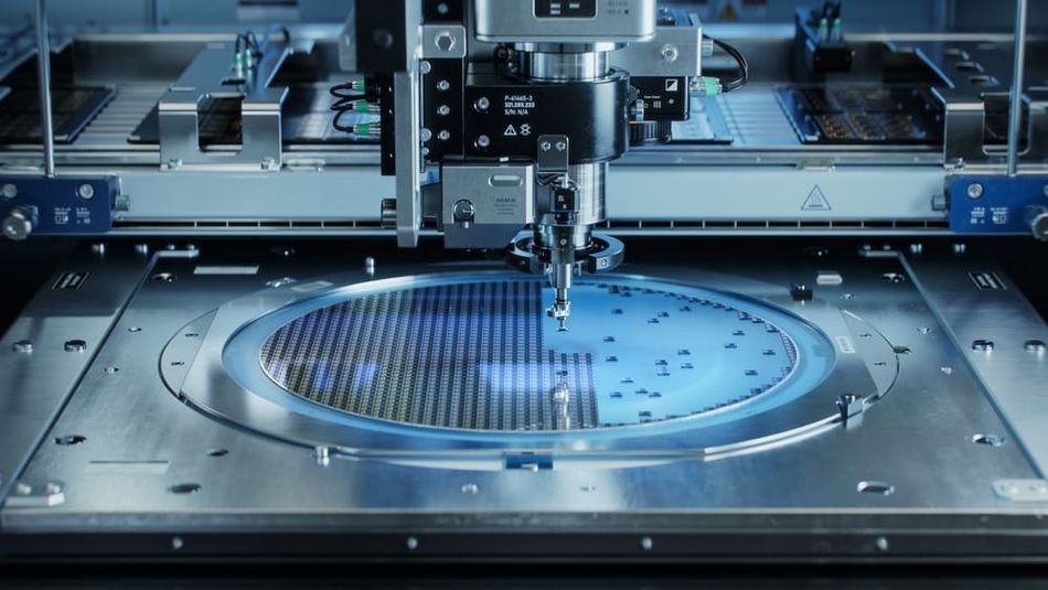
7. Wafer Dicing Equipment and Tooling:
To achieve high-quality dicing results, it is crucial to select the appropriate wafer dicing equipment and tooling. The proper equipment ensures that semiconductor wafers are diced efficiently and accurately, while minimizing damage and maximizing yield. This section discusses various wafer dicing equipment and tooling options available for different dicing techniques.
7.1. Types of Dicing Saws and Blades:
Dicing saws and blades play a critical role in the wafer dicing process, particularly in blade dicing techniques. These tools must be carefully selected to ensure optimal performance and compatibility with the material being diced.
Mechanical dicing saws:
Mechanical dicing saws are the most common type of saw used in blade dicing. They typically employ high-speed spindle rotation and precise linear motion systems to guide the dicing blade through the semiconductor wafer. Mechanical dicing saws can be equipped with various blade types to suit the specific dicing requirements, such as cutting speed, kerf width, and material compatibility.
Diamond dicing blades:
Diamond dicing blades are the most widely used type of blade in the wafer dicing process, due to their excellent cutting performance and durability. They consist of a steel core coated with diamond abrasive particles, which provide the necessary cutting action. Diamond dicing blades come in various designs, such as hubbed or hubless, and can be tailored with different diamond grit sizes, concentrations, and bonding materials to optimize their performance for specific applications.
Resin-bonded dicing blades:
Resin-bonded dicing blades are another type of blade commonly used in wafer dicing. These blades consist of a steel core coated with a resin-based bonding material, which holds the abrasive particles, such as diamond or silicon carbide. Resin-bonded blades offer advantages in certain applications, such as a lower cutting force, reduced chipping, and improved surface quality. However, they typically have a shorter service life compared to diamond dicing blades.
Sintered metal-bonded dicing blades:
Sintered metal-bonded dicing blades are made by sintering a mixture of metal powders and abrasive particles, such as diamond or cubic boron nitride, under high pressure and temperature. This process results in a robust and wear-resistant cutting edge. Sintered metal-bonded blades are particularly suitable for dicing hard and brittle materials, such as silicon carbide or sapphire, as they provide excellent cutting performance and extended blade life.
The choice of dicing saws and blades significantly impacts the quality and efficiency of the wafer dicing process.
7.2. Laser Dicing Systems and Components:
Laser dicing systems have become increasingly popular in the semiconductor industry due to their precise, non-contact cutting capabilities and the ability to process a wide range of materials. These systems typically comprise several key components that work together to deliver efficient and accurate dicing results. In this section, we will explore the main elements of laser dicing systems and their respective functions.
Laser source:
The laser source is the heart of any laser dicing system. It generates the laser beam that is used for cutting the semiconductor wafer. There are several types of laser sources available, each offering specific advantages depending on the material and application requirements. Common laser types used in dicing include CO2, Nd:YAG, and ultrashort pulse lasers, such as femtosecond and picosecond lasers. The choice of laser source depends on factors like the required cutting speed, kerf width, and thermal effects on the material.
Optical system:
The optical system is responsible for directing and shaping the laser beam as it travels from the laser source to the workpiece. This system typically includes components such as mirrors, lenses, and beam expanders, which serve to focus and manipulate the beam for optimal cutting performance. The optical system's design and quality play a crucial role in ensuring precise and efficient material removal during the dicing process.
Motion control system:
The motion control system ensures the accurate positioning and movement of the laser beam relative to the workpiece. It typically consists of high-precision linear stages, rotary stages, and other positioning components, along with a control system that translates the desired cutting pattern into precise movements. The motion control system's accuracy and repeatability are critical factors in achieving high-quality dicing results and maintaining tight tolerances.
Cooling system:
Laser dicing generates heat due to the absorption of laser energy by the workpiece. To prevent overheating and maintain stable operating conditions, a cooling system is integrated into the laser dicing equipment. This system can include components like chillers, heat exchangers, and cooling circuits, which work together to dissipate excess heat and maintain the laser source and other system components within their specified temperature ranges.
Machine vision and inspection system:
A machine vision and inspection system is often integrated into laser dicing equipment to monitor the cutting process in real-time and ensure the quality of the diced dies. This system may include high-resolution cameras, image processing software, and various sensors that can detect and analyze various process parameters, such as kerf width, die placement, and cutting depth. By providing real-time feedback, the machine vision system enables operators to make adjustments and corrections as needed to optimize the dicing process and maintain consistent quality.
7.3. Plasma Dicing Equipment and Gases:
Plasma dicing, also known as plasma etching, is an advanced technique that uses plasma to selectively remove material from a semiconductor wafer, resulting in cleanly diced dies. In this section, we will discuss the key components of plasma dicing equipment and the role of different gases in the process.
Plasma reactor:
The plasma reactor, also known as the etch chamber, is the central component of plasma dicing equipment. It is a closed, vacuum-sealed container where the plasma is generated and the dicing process takes place. The reactor is designed to maintain a controlled environment and provide optimal conditions for plasma generation and etching. It is typically equipped with a wafer holder, temperature control systems, and gas inlets to introduce the necessary gases for the process.
RF power supply and electrodes:
Plasma dicing relies on the generation of plasma, which requires a power source to ionize the gas inside the reactor. The radio frequency (RF) power supply provides the necessary energy to create plasma by applying an electric field to the gas. The RF power supply is connected to electrodes inside the reactor, which create an oscillating electric field that ionizes the gas molecules, forming a plasma. The selection of the appropriate power supply and electrode configuration is crucial for generating a stable and uniform plasma suitable for etching.
Gas supply and flow control:
Different gases are used in plasma dicing to achieve the desired etching characteristics. The choice of gas depends on the material being diced and the specific process requirements. Common gases used in plasma dicing include reactive gases such as sulfur hexafluoride (SF6), chlorine (Cl2), and boron trichloride (BCl3), as well as inert gases like argon (Ar) and nitrogen (N2). The gas supply system includes gas cylinders, regulators, mass flow controllers, and valves to ensure precise control over the gas flow rate and composition during the dicing process.
Exhaust and vacuum system:
Maintaining a low-pressure environment inside the plasma reactor is essential for the generation and stability of plasma. The exhaust and vacuum system is responsible for removing the gaseous byproducts of the etching process and maintaining the desired pressure inside the reactor. This system typically includes vacuum pumps, pressure gauges, and exhaust lines, which work together to create and maintain a controlled environment suitable for plasma dicing.
Control and monitoring system:
The control and monitoring system is responsible for managing the various components of the plasma dicing equipment and ensuring that the process parameters remain within the desired range. This system typically includes a computer or programmable logic controller (PLC) that communicates with sensors, actuators, and other components to control the plasma generation, gas flow, temperature, and pressure during the dicing process. The monitoring system may also include diagnostic tools, such as optical emission spectroscopy (OES) or mass spectrometry, to analyze the plasma composition and process conditions in real-time.
By understanding the essential components of plasma dicing equipment and the role of various gases in the process, manufacturers can optimize their dicing processes
8. Wafer Dicing Process Optimization:
Optimizing the wafer dicing process is crucial for semiconductor manufacturers to achieve higher yields, reduce costs, and improve product quality. Several factors can impact the efficiency and precision of the dicing process, including equipment settings, process parameters, and material properties. In this section, we discuss various strategies and considerations for optimizing the wafer dicing process.
Equipment calibration and maintenance:
Proper calibration and maintenance of dicing equipment are essential for ensuring consistent performance and achieving the desired die quality. Regular calibration of dicing saws, laser systems, and plasma reactors helps maintain the accuracy and precision of the equipment. Additionally, routine maintenance, such as cleaning and replacing worn components like saw blades or electrodes, can prevent process variability and reduce the likelihood of defects.
Selection of dicing method and parameters:
Choosing the most suitable dicing method and process parameters for a specific wafer material and application is crucial for achieving optimal results. Factors such as material properties, die size, and required throughput should be considered when selecting between mechanical, laser, or plasma dicing techniques. Additionally, adjusting process parameters like cutting speed, feed rate, and laser pulse duration can help balance the trade-offs between precision, quality, and throughput.
Material characterization and analysis:
Understanding the material properties of the wafer and any related films or coatings is essential for optimizing the dicing process. Material properties, such as hardness, fracture toughness, and thermal conductivity, can influence the choice of dicing method and the required process parameters. Conducting material characterization techniques like X-ray diffraction (XRD), scanning electron microscopy (SEM), or atomic force microscopy (AFM) can provide valuable insights into the material properties and help identify potential challenges and solutions for the dicing process.
Process monitoring and feedback control:
Implementing process monitoring and feedback control systems can help semiconductor manufacturers identify and correct process deviations in real-time. Monitoring techniques such as optical emission spectroscopy (OES) for plasma dicing or laser interferometry for mechanical dicing can provide real-time data on process conditions and equipment performance. Integrating these monitoring techniques with feedback control systems allows for the automatic adjustment of process parameters, ensuring consistent performance and minimizing the occurrence of defects.
Design for manufacturability (DFM):
Considering wafer dicing requirements during the design stage of semiconductor devices can lead to improved dicing outcomes and increased manufacturing efficiency. Design for manufacturability (DFM) principles, such as incorporating stress relief features like scribe lines or trenches and optimizing die layout for dicing efficiency, can help minimize potential issues during the dicing process and improve die yield.
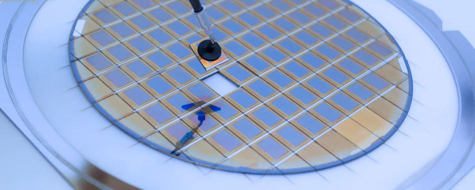
9. Quality Control and Inspection in Wafer Dicing:
Rigorous inspection procedures for quality control in wafer dicing can help identify defects, improve process efficiency, and minimize waste. In this section, we discuss various quality control and inspection techniques used in the wafer dicing process.
Automated Optical Inspection (AOI):
Automated Optical Inspection (AOI) is a widely used inspection technique in semiconductor manufacturing, which involves capturing high-resolution images of the wafer surface using cameras and analyzing them using image processing algorithms. AOI can detect a variety of defects, such as chipping, delamination, and contamination, by comparing the captured images against predefined criteria. With rapid data acquisition and analysis capabilities, AOI systems can quickly identify and classify defects, allowing for prompt corrective actions.
Scanning Acoustic Microscopy (SAM):
Scanning Acoustic Microscopy (SAM) is a non-destructive inspection technique that uses high-frequency ultrasound waves to probe the internal structure of the wafer and detect hidden defects, such as voids, cracks, and delaminations. SAM generates an acoustic image of the wafer by measuring the intensity of the reflected ultrasound waves at different depths. This technique can reveal defects that are not visible through optical inspection methods, providing valuable information for process improvement and quality control.
In-line metrology and process control:
In-line metrology and process control techniques involve monitoring the wafer dicing process in real-time and collecting data on process parameters, such as cutting speed, feed rate, and laser power. By continuously monitoring these parameters and integrating them with feedback control systems, semiconductor manufacturers can maintain consistent process conditions, minimize variability, and improve overall product quality.
Die strength and reliability testing:
Die strength and reliability testing are essential for ensuring the mechanical and functional integrity of semiconductor devices. Tests such as wire pull, die shear, and thermal cycling can provide information on the mechanical strength, bond quality, and thermal performance of the die. These tests help identify potential weaknesses in the dicing process, enabling manufacturers to make necessary adjustments and improvements.
Statistical Process Control (SPC):
Statistical Process Control (SPC) is a methodology for analyzing and controlling the wafer dicing process using statistical techniques. By collecting data on process parameters and defect rates, SPC allows manufacturers to identify trends, patterns, and sources of variability, enabling them to make data-driven decisions for process improvement. SPC tools, such as control charts and process capability indices, can help manufacturers maintain process stability, reduce defects, and improve overall product quality.
10. Conclusion
The wafer dicing process is a critical step in the semiconductor manufacturing process, where the semiconductor wafer is cut into individual dies, each containing a fully functional integrated circuit. The evolution of semiconductor devices, driven by the need for smaller, faster, and more energy-efficient components, has led to advancements in wafer dicing technologies and techniques. These developments have focused on addressing challenges such as die chipping and breakage, contamination and cleanliness, and precision and accuracy, while improving the overall efficiency of the dicing process.
Innovative approaches to wafer dicing, such as advanced laser dicing systems and novel dicing techniques and materials, have allowed for higher precision, reduced damage, and increased throughput. Equipment and tooling innovations, including different types of dicing saws and blades, laser dicing systems and components, and plasma dicing equipment and gases, are also essential in achieving superior quality and performance in semiconductor devices.
Optimizing the wafer dicing process and implementing rigorous quality control and inspection methods, such as Automated Optical Inspection (AOI), Scanning Acoustic Microscopy (SAM), in-line metrology, and Statistical Process Control (SPC), can further enhance product quality and yield rates. Through continuous improvement and innovation, the semiconductor industry can meet the ever-growing demands for advanced electronic devices that power our modern world.
11. Frequently Asked Questions (FAQs)
1: What is wafer dicing?
Wafer dicing is a process in semiconductor manufacturing where a thin, circular wafer containing multiple integrated circuits is cut into individual dies or chips. Each die contains a fully functional integrated circuit, which can be packaged and used in electronic devices.
2: What are the main challenges faced during the wafer dicing process?
The primary challenges faced during wafer dicing include die chipping and breakage, contamination and cleanliness, and precision and accuracy. Addressing these challenges is essential to ensuring high-quality semiconductor devices and maximizing yield rates.
3: What are some innovations in wafer dicing technology?
Innovations in wafer dicing technology include advanced laser dicing systems, novel dicing techniques and materials, and the development of new equipment and tooling, such as specialized dicing saws and blades, laser dicing systems and components, and plasma dicing equipment and gases.
4: How is quality control and inspection performed in wafer dicing?
Quality control and inspection in wafer dicing involve various techniques, such as Automated Optical Inspection (AOI), Scanning Acoustic Microscopy (SAM), in-line metrology and process control, die strength and reliability testing, and Statistical Process Control (SPC). These methods help ensure the production of high-quality, reliable semiconductor devices by identifying defects, monitoring process parameters, and implementing continuous improvement strategies.
5: What factors influence the choice of dicing method for a particular semiconductor application?
Factors that influence the choice of dicing method include the material properties of the wafer, the dimensions and features of the integrated circuits, the required precision and accuracy, the desired throughput, and the overall cost of the dicing process. Different dicing methods, such as mechanical dicing, laser dicing, and plasma dicing, offer varying levels of performance and cost-effectiveness, depending on the specific requirements of the semiconductor application.
References:
https://sst.semiconductor-digest.com/2007/03/wafer-dicing-a-sticky-situation/
https://www.thomasnet.com/articles/custom-manufacturing-fabricating/wafer-dicing/
in this article
1. Introduction to Wafer Dicing1. What are Semiconductor Wafers? 2. Why Dicing is Important in Semiconductor Manufacturing?3. Common Wafer Dicing Techniques4. Factors to Consider When Choosing a Dicing Technique:5. Wafer Dicing Challenges and Solutions:6. Innovations in Wafer Dicing Technology:7. Wafer Dicing Equipment and Tooling:8. Wafer Dicing Process Optimization:9. Quality Control and Inspection in Wafer Dicing:10. Conclusion11. Frequently Asked Questions (FAQs)13. References: