


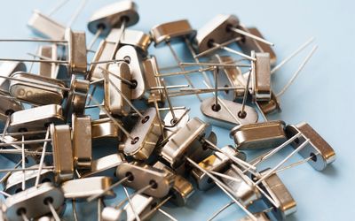
A crystal oscillator is an electronic circuit that uses a quartz crystal to produce a precise and stable frequency reference. This article covers crystal operation, equivalent circuit models, resonance, load capacitance, oscillator topologies, stability, aging, and design practices.
Be the first to know.
Get our semiconductors weekly email digest.
Tagged with
semiconductors
ORGANIZATIONS. SHAPING THE INDUSTRY.


Nordic Semiconductor
Semiconductors
Nordic Semiconductor is a fabless semiconductor company specializing in wireless technology that powers the IoT.
181 Posts

Intrinsic ID
Semiconductor
Securing the IoT with the World's Top PUF Technology. Authenticate Everythi...
16 Posts
Latest Posts

Master the Bandgap Voltage Reference — understand the physics, compare popular topologies, explore real-world applications, and choose the right IC for your analog design. A practical guide for engineers.


Nexperia links device-level advantages to application requirements, helping designers choose the best Wide bandgap (WBG) solution for their design.

Rising power demands from emerging industries are pushing manufacturers to maximize the performance and efficiency of their power supplies. Using advanced power semiconductor packaging technologies is becoming essential to meet the next-gen targets.


Physics is about the web, rather than the spider.

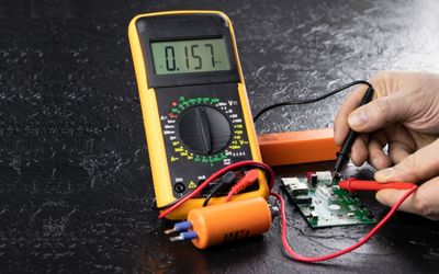
Learn how to use a multimeter with engineering-grade precision. This technical guide explores advanced measurement techniques, safety CAT ratings, and error minimization strategies for high-fidelity diagnostics.

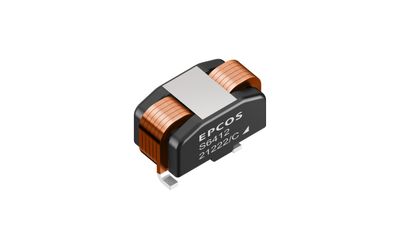
Discover how the ERUC23 coupled inductor enables compact, high-efficiency multiphase power systems with reduced ripple, lower losses, and improved thermal management.

The new framework replaces approximations, accurately modeling current crowding and spreading resistance in 2D materials to improve high-performance semiconductor devices.

4 minutes read

Explore Business Tai Chi, a values-first model for deep-tech companies that balances financial sustainability, engineering learning, and team alignment to build resilient semiconductor innovation.


Hybrid bonding provides the adhesive free, copper to copper interconnects that are driving cutting edge 3D chip stacking. This article explains the theory, process, benefits, challenges, applications, and emerging trends of hybrid bonding for engineers.

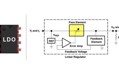
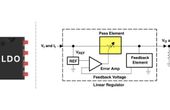
This article explains what is LDO, how the LDO regulator works, discusses key specifications such as dropout voltage, line/load regulation, noise, and PSRR, and shows how to select and design with LDOs to meet demanding engineering requirements.

Soldering wires is the process of joining electrical conductors using a melted filler metal to create strong, low-resistance connections. This guide explains tools, techniques, heat control, materials, common defects, and engineering best practices for reliable electrical connections.

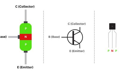
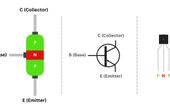
This article focuses on the PNP transistor, exploring its structure, physics, operating modes, differences from its NPN counterpart, and how to design reliable switching, amplification, and power management circuits using it.

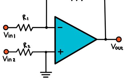
An operational amplifier (op-amp) is a high-gain differential amplifier used in analog circuitry to process and condition signals. This article examines op-amp theory, ideal and real behavior, key specifications, core circuits, applications, and practical design considerations.
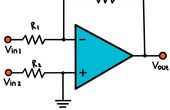
A non-inverting amplifier is an op-amp configuration that delivers in-phase voltage gain with high input impedance. This article explains its theory, schematic symbols, gain calculation, bandwidth limits, noise, stability trade-offs, and real-world design practices.
