FPGA Programming: Theory, Workflow, and Practical Implementations
Explore the fundamentals of FPGA programming, step-by-step design flow, HDL choices, and practical techniques used by digital designers and hardware engineers to build efficient, real-world digital systems.

01 Dec, 2025. 13 minutes read
Key Takeaways
- Foundational understanding: Learn how FPGAs are configurable integrated circuits with arrays of programmable logic blocks that can be repeatedly programmed for diverse applications.
- Design flow: Familiarize yourself with the seven‑step FPGA design flow—design entry, simulation, synthesis, placement, routing, configuration file generation, and final configuration.
- Language choices: Grasp differences between Verilog and VHDL; Verilog’s concise syntax is easier for programmers, whereas VHDL’s strongly typed structure promotes disciplined design.
- Practical insights: Explore high‑level synthesis, debugging strategies, optimization tips, and real‑world examples across industries such as telecommunications, automotive, and healthcare.
- Future trends: Understand how increasing FPGA capacity, AI accelerators, and open‑source toolchains are reshaping development and enabling rapid prototyping.
Introduction
Field‑programmable gate arrays (FPGAs) have revolutionised digital design by letting engineers build customized hardware logic that can be reconfigured after manufacturing. Unlike CPUs that execute sequential instructions, FPGAs consist of arrays of configurable logic blocks connected via programmable routing. These devices enable true massively parallel computation and deterministic timing, making FPGAs essential in high‑performance computing, embedded systems, and prototyping.
The popularity of FPGA programming has increased with advances in development toolchains and high‑level synthesis (HLS), which enable software-focused developers to describe complex hardware functionality without dealing with low-level implementation details. But effective use of FPGAs still requires understanding digital design fundamentals, hardware description languages (HDLs), timing constraints, and resource management. This article provides a deep dive into both theoretical and practical aspects of FPGA programming to help engineers and students build efficient designs for real‑world applications.
We begin by reviewing the architecture and theoretical concepts underlying FPGAs, then move into design flows, language choices, debugging techniques, and high‑level synthesis. A comparative table summarises popular HDLs, and a step‑by‑step practical example illustrates how to turn an algorithm into an FPGA implementation. We conclude with FAQs and resources to support further learning.
1. Theoretical Foundations of FPGA Programming
1.1 What Is an FPGA?
A field‑programmable gate array (FPGA) is a type of configurable integrated circuit that can be repeatedly programmed after manufacturing [1]. FPGAs are a subset of programmable logic devices (PLDs), which also include CPLDs—smaller, simpler devices suited for glue logic and control tasks. They consist of a grid of programmable logic blocks, routing resources, and input/output (I/O) blocks. These blocks can be configured to implement virtually any digital circuit.
Key features of FPGAs include:
Reconfigurability: Unlike ASICs, FPGAs can be reprogrammed multiple times. This enables rapid prototyping and iterative development.
Parallelism: The array of logic blocks enables true parallel execution, resulting in achieving high throughput and deterministic timing.
Flexibility: FPGAs support various logic functions, from simple gates to complex finite‑state machines (FSMs) and DSP blocks.
Embedded resources: Modern devices incorporate memory blocks (RAM), DSP slices, phase‑locked loops (PLLs), and high‑speed transceivers for enhanced computation and communication capabilities.
FPGAs are used in telecommunications, automotive systems, aerospace, industrial automation, and research, where engineers build a wide range of FPGA projects on a single FPGA device. They enable on‑the‑fly algorithm changes, hardware acceleration, and low‑latency signal processing, making them ideal for both commercial systems and academic FPGA projects. A design is typically described using an HDL such as VHDL or Verilog, synthesized into a netlist, and mapped onto the FPGA’s resources before being stored in flash memory for device configuration [1].
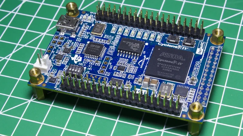
Beginners typically start experimenting on an FPGA development board, which provides I/O headers, configuration interfaces, and debug features for hands-on learning.
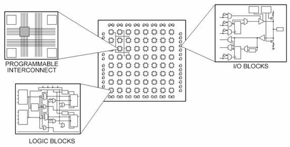
1.2 FPGA Architecture
Understanding the internal architecture of an FPGA is critical for effective programming. The main architectural components of an FPGA are:
Configurable Logic Blocks (CLBs): Each CLB contains look‑up tables (LUTs), multiplexers, and flip‑flop elements. LUTs implement combinational logic, while flip‑flops provide sequential storage.
Routing Resources: FPGAs contain a hierarchy of routing resources—local, intermediate, and global interconnects, which are used to connect CLBs, embedded blocks, and I/O blocks. The routing fabric determines how signals travel across the device, influencing delay and overall performance. Effective placement and routing help ensure timing closure and prevent congestion in high-density designs.
I/O Blocks: These blocks interface with external signals, supporting various standards (e.g., LVDS, PCIe, Ethernet, and general-purpose I/O protocols). Pin assignments are defined during the design phase.
Embedded Blocks: Modern FPGAs integrate on-chip memory (block RAM), DSP slices for high-speed arithmetic operations, clock management units (e.g., PLLs and MMCMs), and sometimes embedded processor systems, most commonly ARM Cortex-A or Cortex-R cores. Popular vendors such as Xilinx and Altera (now part of Intel) offer devices with increasingly advanced embedded resources.
1.3 Digital Logic Fundamentals
FPGA programming is grounded in digital logic theory. Engineers must be comfortable with:
Boolean algebra and truth tables, which underpin all combinational logic.
Combinational circuits such as gates, multiplexers, decoders, encoders, and arithmetic units.
Sequential circuits including (flip‑flops, registers, counters, and finite-state machines (FSMs).
Timing concepts such as propagation delay, setup and hold times, clock skew, and metastability all of which affect the reliability of synchronous designs.
1.4 Hardware Description Languages (HDLs)
HDLs are not programming languages and are used to describe the hardware structure and behaviour of digital hardware. They allow designers to model concurrency, define timing relationships, and create synthesizable logic. The two dominant languages are VHDL and Verilog. Both are standardized and widely supported, but they differ in design philosophy, typical use cases, and syntax:
Verilog: Originating in the 1980s, Verilog has a concise syntax similar to C [2]. It supports procedural and concurrent constructs, making it approachable for software programmers. Verilog is popular in ASIC design and industries that prioritize rapid prototyping.
VHDL (Very High‑Speed Integrated Circuit HDL): Developed under a US Department of Defense initiative, VHDL is strongly typed and verbose [2]. Its explicitness enforces discipline, aiding maintainability and reliability. VHDL is widely adopted in safety‑critical domains, such as applications (aerospace, defence, and medical), where rigorous verification and traceability are essential.
Choosing between Verilog and VHDL depends on project requirements, team experience, and industry norms. Many engineers become fluent in both to leverage the strengths of each language. Other HDLs include SystemVerilog (an extension of Verilog), Chisel (Scala‑based), MyHDL (Python‑based), and specialized high‑level languages used in HLS (e.g., C/C++, OpenCL).
1.5 High‑Level Synthesis (HLS)
High‑Level Synthesis tools convert algorithmic descriptions (often in C/C++, SystemC, or OpenCL) into register-transfer level (RTL) code. This approach allows software developers to target FPGAs without writing low‑level HDL. HLS benefits include:
Productivity: HLS accelerates development by enabling rapid prototyping and iterative refinement.
Portability: High‑level models can be easily retargeted across different FPGA families with minimal changes.
Abstraction: Designers can focus on algorithms rather than gates and wires while the tool handles resource allocation, scheduling, and pipelining.
Even with these benefits, HLS still requires a strong understanding of hardware concepts to produce efficient designs. Pragmas and directives are used to control loop unrolling, pipelining, and resource sharing.Post‑HLS optimization may be needed to meet performance, timing, and resource utilization goals.
Recommended Reading: ASIC vs FPGA: A Comprehensive Comparison
2. FPGA Design Flow: From Idea to Bitstream
Developing FPGA designs follows a structured workflow that spans specification through implementation. This section outlines each step, emphasising tasks, recommended tools, and industry best practices.
2.1 Design Entry
The first step is writing the desired hardware functionality in an HDL. According to a practical guide, design entry often involves writing VHDL or Verilog in a text editor and is often the most time‑consuming stage [3]. Good coding practices, such as modular design, use of generics/parameters, and adherence to naming conventions, ease maintenance and reuse.
For simple designs, schematic entry may suffice; however, text‑based HDL is better suited for complex, scalable systems. Version control systems like Git help in managing changes, tracking revisions, and enabling collaboration in team-based projects.
2.2 Functional Simulation
Before synthesis, the design is simulated to verify functional correctness. Engineers create testbenches that apply input stimuli and check expected outputs. Simulation helps catch logical errors early. Tools such as ModelSim, QuestaSim, and Vivado Simulator support both behavioural and timing-level simulation.
2.3 Design Synthesis
Synthesis converts high‑level HDL code into a technology‑specific netlist. The netlist maps logic to LUTs, flip‑flops, and other resources. Synthesis tools perform optimizations like logic minimization, resource sharing, and retiming. In the example from FPGATek, synthesis translates behavioural descriptions into LUT-based implementations [3]. Key considerations include:
Timing constraints: Use constraints files (e.g., .xdc for Vivado) to specify clock frequencies and input/output delays. Failing to meet timing at this stage may require code restructuring.
Resource utilisation: Analyse synthesis reports to ensure LUTs, BRAM, and DSP counts fit the target device.
2.4 Placement
Placement determines where each logical element (e.g., LUTs, registers) will reside physically on the FPGA. As FPGATek explains, engineers assign which specific resource in the FPGA will implement the design [3]. Good placement strategies consider clock domains and minimize routing congestion. Tools automatically place components, but manual floorplanning may be necessary for complex designs.
2.5 Routing
Routing connects the placed elements via programmable interconnects. The routing algorithm selects paths between resources, balancing delay, path length, and congestion. The design must satisfy timing constraints; if not, the tool may reattempt routing or the designer may need to adjust constraints or modify the architecture. Efficient routing is essential for meeting target clock frequencies and minimizing latency [3].
2.6 Configuration File Generation
Once placement and routing are complete, a configuration (bitstream) file is generated. This bitstream encodes the logic and routing information to program the FPGA. Tools like Xilinx Vivado or Intel Quartus produce bitstreams. It's important to use the correct version for the target FPGA family.
2.7 Device Programming and Testing
Load the bitstream onto the FPGA via JTAG, USB, or other interfaces. After programming, perform hardware testing with real or simulated inputs. This stage is iterative; engineers often cycle back to simulation and synthesis to fix issues discovered during hardware testing. FPGA development tools provide integrated debugging features, such as Logic Analyzers (ILA in Vivado) and Virtual I/O modules, to aid verification and troubleshooting.
3. Choosing Hardware Description Languages
HDL choice influences design methodology, readability, and verification. The table below compares popular languages.
Language | Strengths | Typical Use Cases |
VHDL | Strong typing; explicit structure; high maintainability [2]. | Aerospace, defence, medical devices, and education |
Verilog | Concise syntax; familiar to C programmers; quick development [2]. | ASIC design, prototyping, mixed‑language environments |
SystemVerilog | Extends Verilog with advanced verification constructs, classes, and assertions | Complex designs requiring verification, testbenches |
Chisel | Hardware construction language built on Scala; supports parameterization and generators | Research, RISC‑V cores, flexible architectures |
MyHDL | Python‑based; converts Python code to VHDL/Verilog; fosters algorithmic description | Education, quick prototyping |
HLS (C/C++, OpenCL) | High‑level abstractions; auto‑generates RTL; increases productivity | Algorithm acceleration, AI/ML, data processing |
3.1 Verilog and VHDL in Depth
This subsection covers the two most widely used HDLs, Verilog and VHDL, which dominate the FPGA design. Other languages are summarized in the previous table.
Verilog models hardware using modules, always blocks, and assign statements. Its syntax includes continuous and procedural assignments, supporting. It supports four‑value logic (0, 1, X, Z). Advantages include a shorter learning curve for software engineers and broad industry support. However, its weaker typing may allow accidental cross‑type operations, leading to subtle bugs if not carefully managed [2].
VHDL emphasises strong typing, explicit concurrency, and modularity. It uses entities and architectures to separate interface from implementation. Its libraries (e.g., ieee.std_logic_1164) define standard logic types with additional states (U, X, 0, 1, Z, W, L, H, –). VHDL’s verbosity encourages thorough documentation and reduces ambiguity. The steep learning curve pays off in large‑scale projects and regulated industries.
3.2 Mixed‑Language Design
Most modern FPGA tools support mixed‑language design—allowing Verilog modules to be instantiated in a VHDL top level or vice versa. This approach facilitates IP reuse across languages and lets teams leverage domain-specific expertise. This allows reuse of IP cores regardless of the original language and enables teams to leverage domain expertise.
4. Practical Implementation: Building a Universal Counter
To illustrate the complete workflow, we’ll implement an 8‑bit universal counter using VHDL, drawing on the codilime example [4]. This design features load, enable, and reset inputs, demonstrating combinational and sequential logic.
4.1 Specification
Inputs: clk, rst, load, enable, input (8‑bit).
Output: output (8‑bit).
Functionality: When rst is asserted, the counter resets to zero. If the load is high, the counter loads the input value. If enable is high, the counter increments at each clock cycle; otherwise, it retains its value.
4.2 VHDL Code Snippet
library ieee;
use ieee.std_logic_1164.all;
use ieee.numeric_std.all;

entity universal_counter is
  generic (BIT_WIDTH : integer := 8);
  port (
    clk    : in std_logic;
    rst    : in std_logic;
    load   : in std_logic;
    enable : in std_logic;
    input  : in std_logic_vector((BIT_WIDTH-1) downto 0);
    output : out std_logic_vector((BIT_WIDTH-1) downto 0)
  );
end universal_counter;

architecture rtl of universal_counter is
  signal value_r, value_next : unsigned((BIT_WIDTH-1) downto 0);
begin
  process(clk, rst)
  begin
    if rst = '1' then
      value_r <= (others => '0');
    elsif rising_edge(clk) then
      value_r <= value_next;
    end if;
  end process;

  -- Next value logic
  value_next <= unsigned(input) when load = '1' else
                value_r + 1 when enable = '1' else
                value_r;


  output <= std_logic_vector(value_r);
end rtl;
This architecture defines internal signals value_r (current count) and value_next (next count), updating them on rising clock edges. The generic parameters allow easy scaling of bit width.
4.3 Simulation
Use a testbench to stimulate the counter across scenarios—reset assertion, loading different input values, enabling counting, and disabling counting. Verify waveforms to ensure correct operation under various conditions.
4.4 Synthesis, Placement, and Routing
After functional simulation passes, synthesise the design using a tool like Vivado:
Synthesis: Generate a netlist and review resource utilization. The counter uses minimal LUTs and flip‑flops.
Placement: Let the tool assign specific LUTs and flip‑flops. In larger designs, manual placement might optimize timing.
Routing: Ensure routing meets timing constraints. If not, consider pipelining or retiming.
Bitstream Generation: Produce a .bit file for your target FPGA board.
Programming and Testing: Use a development board (e.g., Xilinx Artix‑7) to program the FPGA. Connect inputs via switches or a microcontroller and observe the counter output using LEDs or an analyzer.
4.5 Debugging
If the counter doesn’t behave as expected:
Use an Integrated Logic Analyzer (ILA) to observe internal signals in real time.
Confirm that the constraints files assign the correct pins.
Check for metastability on asynchronous inputs (e.g., load, enable) and synchronise them if necessary.
Ensure reset logic covers all registers.
5. High‑Level Synthesis and Advanced Topics
5.1 High‑Level Synthesis (HLS) Workflow
HLS bridges the gap between software and hardware by compiling algorithmic descriptions into RTL. The general HLS workflow:
Algorithm Specification: Write code in C/C++, SystemC, or OpenCL describing the algorithm.
Synthesis Directive: Annotate loops and functions with directives (pragmas) to control unrolling, pipelining, and resource use.
RTL Generation: The HLS tool generates synthesizable VHDL or Verilog.
Verification: Validate the generated RTL against the original algorithm via co‑simulation.
Implementation: Integrate the RTL into the rest of the design, then proceed with standard synthesis and place‑and‑route.
HLS is well-suited for computational kernels such as filtering, matrix multiplication, and neural-network layers. Tools include Xilinx Vivado HLS, Intel HLS Compiler, and open‑source frameworks such as LegUp and Vitis HLS.
5.2 Partial Reconfiguration
Some FPGAs support partial reconfiguration (PR), enabling sections of the device to be reprogrammed while the rest remains operational. PR allows dynamic swapping of functions (e.g., different accelerators) and reduces downtime. Designing for PR requires careful partitioning of the design into static and reconfigurable regions, along with generating separate partial bitstreams for each configuration.
5.3 Embedded Processors and SoC FPGAs
Many FPGAs include embedded microprocessors (e.g., Xilinx Zynq with ARM Cortex‑A9). These system‑on‑chip (SoC) FPGAs combine programmable logic with processors, DDR controllers, and peripherals. They enable hardware/software co‑design where performance‑critical tasks run in programmable logic and system control runs on the processor. Development tools offer an integrated workflow for managing both the software stack and the hardware fabric.
5.4 Security Considerations
Security is critical because FPGAs may run proprietary or mission-critical algorithms. Measures include:
Bitstream encryption: Encrypt configuration files to protect against reverse-engineering and device cloning.
Authentication: Use digital signatures to ensure only authorized bitstreams can program the device.
Side‑channel protection: Implement measures to mitigate differential power analysis (DPA) and electromagnetic attacks.
Secure boot: Combine the FPGA with a secure processor or root-of-trust to ensure device integrity trust at power‑up.
6. Applications of FPGA Programming
6.1 Telecommunications
FPGAs excel at processing high‑bandwidth signals and implementing algorithms like Fast Fourier Transforms (FFT), forward-error‑correction codes (e.g., LDPC, Turbo), digital up/down conversion, and beamforming. Their reconfigurable nature makes them ideal for evolving standards such as 5G and emerging 6G systems (e.g., 5G/6G).
6.2 Automotive and Industrial Control
In advanced driver‑assistance systems (ADAS), FPGAs provide real‑time sensor fusion, vision processing, and motor control. Industrial automation uses FPGAs for precise timing, deterministic control loops, and safety‑critical functions. Their inherent determinism ensures consistent performance even in harsh operating environments.
6.3 Aerospace and Defence
FPGAs are widely used in radar, communications, satellite systems, and avionics, where reliability, radiation tolerance, and long product lifecycles are essential. VHDL’s strong typing and disciplined design practices are often preferred or required in these sectors [2].
6.4 High‑Performance Computing and AI
With growing demand for hardware accelerators in AI and data analytics, FPGAs offer customizable, energy‑efficient computation. They support custom numeric formats (e.g., INT8, mixed-precision), parallel pipelines, and memory hierarchies tailored to specific models. Recent devices include dedicated AI engines (e.g., AMD Versal AI Core) and HBM memory stacks for data-intensive workloads.
6.5 Finance and Trading
Low‑latency trading systems use FPGAs for deterministic, ultra-low-latency execution times in nanosecond ranges. Tasks such as order book processing, risk checks, and network protocol handling benefit from FPGA offloading, helping firms reduce round-trip latency and gain a competitive edge.
7. Best Practices for Successful FPGA Programming
Start simple: Begin with small modules; verify each before integration.
Write reusable code: Use generics and parameters to create flexible designs.
Modularize: Break complex systems into hierarchical blocks. Each module should have a clear interface and encapsulated functionality.
Constrain properly: Define clock constraints and I/O timing. Use false paths to ignore unconstrained paths.
Simulate thoroughly: Create comprehensive testbenches. Use corner cases and random stimuli to catch hidden bugs.
Review synthesis and implementation reports: Check resource utilisation, timing slack, and warnings.
Document: Comment code, maintain version history, and provide design specifications.
Learn vendor tools: Master your FPGA vendor’s IDE; each has unique flows, scripts, and optimization options.
Stay updated: FPGA technology evolves rapidly. Follow vendor roadmaps, community forums, and training resources.
Conclusion
FPGA programming is a powerful skill bridging software and hardware engineering. By understanding the theoretical foundations—programmable logic arrays, digital design principles, and HDLs—and following a structured design flow, engineers can harness the parallelism and flexibility of FPGAs for a wide range of applications. Modern innovations like high‑level synthesis (HLS), partial reconfiguration, and integrated processors expand the reach of FPGAs into new domains.
The choice of HDL, whether Verilog or VHDL, depends on project needs, team expertise, and industry norms. Evolving toolchains, improved simulation environments, and growing HLS adoption are lowering the barrier to entry, making hardware design more accessible to software-centric developers and enabling rapid prototyping and deployment.
As demand for custom accelerators grows in AI, telecommunications, and embedded systems, FPGA programming will remain a critical competency for digital design engineers, hardware engineers, and electronics students.
Frequently Asked Questions
Q1: What is FPGA programming?
FPGA programming refers to configuring the logic blocks and routing resources of a field‑programmable gate array to implement a desired digital circuit. Unlike programming a CPU, there is no sequential program; instead, you describe hardware behaviour using an HDL. The building blocks are logic gates, adders, registers, and multiplexers [4].
Q2: Which language should I learn first—VHDL or Verilog?
If you come from a software background, Verilog’s concise, C‑like syntax may be more intuitive. VHDL enforces strong typing and explicitness, which encourages disciplined design and is favoured in regulated industries [2]. Learning both is advantageous.
Q3: How does FPGA design differ from ASIC design?
ASICs are custom integrated circuits fabricated for a specific function. FPGAs are reprogrammable and suitable for low to medium‑volume applications, prototyping, and evolving standards. ASICs offer lower per‑unit cost and power at large volumes but require longer development cycles and higher non‑recurring engineering costs.
Q4: What tools are needed for FPGA development?
You need an HDL editor (e.g., built into vendor tools), synthesis tool, place‑and‑route tool, and simulator. Vendors provide integrated suites like Xilinx Vivado, AMD Vitis, and Intel Quartus. Additional tools include logic analyzers, HLS compilers, and version control systems.
Q5: Can I program FPGAs using high‑level languages like Python or C++?
Yes. High‑level synthesis tools convert C/C++, SystemC, or OpenCL into HDL. Frameworks like MyHDL enable writing Python that translates to Verilog or VHDL. HLS accelerates development but still requires an understanding of hardware concepts to achieve efficient implementations.
Q6: What are common mistakes beginners make?
Common pitfalls include neglecting clock domain crossing issues, misusing blocking/nonblocking assignments (in Verilog), failing to properly constrain timing, overlooking metastability risks, and treating HDL code as if it runs sequentially rather than in parallel. Beginners also tend to skip simulation or ignore synthesis and timing warnings, which often leads to hard-to-trace hardware bugs. Thorough simulation and careful reading of synthesis warnings help avoid these errors.
Q7: Where can I learn more about FPGA programming?
Good resources include vendor documentation, online courses, open‑source projects, community forums, and textbooks. The FPGATek design flow guide describes the seven‑step process from design entry to configuration [3]. The codilime tutorial provides an introduction to HDL programming and examples [4]. Academic courses and workshops offer hands‑on experience.
References
[1] "Field-programmable gate array," Wikipedia, Nov. 25, 2025. [Online]. Available: https://en.wikipedia.org/wiki/Field-programmable_gate_array. [Accessed: Nov. 27, 2025].
[2] "Verilog vs VHDL: Choosing the Right HDL for FPGA Design," BLT Inc., May 27, 2025. [Online]. Available: https://bltinc.com/2025/05/27/verilog-vhdl/. [Accessed: Nov. 27, 2025].
[3] "FPGA Design Flow — From Idea to Bitstream," FPGATek. [Online]. Available: https://fpgatek.com/fpga-design-flow/. [Accessed: Nov. 27, 2025].
[4] M. Trochimiuk, “FPGA programming — introduction guide to HDL,” CodiLime Blog, Aug. 3, 2022. [Online]. Available: https://codilime.com/blog/fpga-programming/ [Accessed: Nov. 27, 2025].
in this article
1. Introduction1. Theoretical Foundations of FPGA Programming2. FPGA Design Flow: From Idea to Bitstream3. Choosing Hardware Description Languages4. Practical Implementation: Building a Universal Counter5. High‑Level Synthesis and Advanced Topics6. Applications of FPGA Programming7. Best Practices for Successful FPGA Programming9. Conclusion10. Frequently Asked Questions11. References