Full Adder Circuit: Theory, Design and Practical Implementation
Learn everything you need about the full adder circuit. From binary addition theory to low-power hardware implementations and modern ASIC/FPGA design flows, this technical article equips digital design engineers, hardware engineers with practical insights and current research trends.

03 Dec, 2025. 12 minutes read

Key takeaways
A full adder circuit adds three binary inputs (two data bits and a carry-in) and produces a sum and carry-out. It can be built using XOR, AND, and OR gates and is more versatile than a half adder.
Two half adders with an extra OR gate can implement a full adder. It’s implementation is also possible with universal logic using only NAND or NOR gates.
Cascading full adders creates ripple carry adders; carry look-ahead adders and other architectures reduce propagation delay by computing carry bits in parallel.
Standard ICs such as the 74LS83/74HC83 integrate four full adders with fast carry logic; modern low-power designs use Gate Diffusion Input (GDI) techniques to reduce power and area by up to 55 %.
Full adder circuits form the core of arithmetic logic units (ALUs), address generators and multiplication circuits.
Introduction
Binary arithmetic is the core operational element in every digital device, ranging from microcontrollers in household appliances to multi-core processors in data centres. A full adder circuit lies at the heart of binary arithmetic. It’s a combinational logic network that adds three input bits and produces a two-bit result—sum and carry. Full adders are very simple in concept. The design of a full adder and its integration into larger arithmetic units involves important trade-offs in terms of:
speed
Power
Area
Scalability
Therefore, engineers working with digital logic must understand how a full adder works, how it differs from a half adder, how to build it using basic gates or hardware description languages, and how modern research pushes its performance limits.
This article discusses a holistic view of the full adder circuit. We will discuss the theory of binary addition and the differences between half- and full-adders. Later, we will cover several implementation strategies—from gate-level schematics and transistor-level realisations to high-level hardware design flows for FPGAs and ASICs. The discussion extends to multi-bit architectures, such as ripple-carry and carry-look-ahead adders, and highlights commercial ICs as well as low-power innovations.
Binary Addition - Why Do We Need a Full Adder?
Digital systems represent numbers in base-2, where each bit can be 0 or 1. It means that a carry may be generated during bit-by-bit addition.
The simplest adder is a half adder, which adds two single-bit inputs but cannot handle a carry-in from a previous addition. Its output comprises a sum and a carry bit. A full adder was developed to tackle the carry problem in multi-bit addition.
Half adder vs full adder
The main differences between a half adder and a full adder are summarised in the table below. Each keyword entry is kept short to fit within narrow columns. In a half adder, the sum is the XOR of A and B and the carry is the AND of A and B.
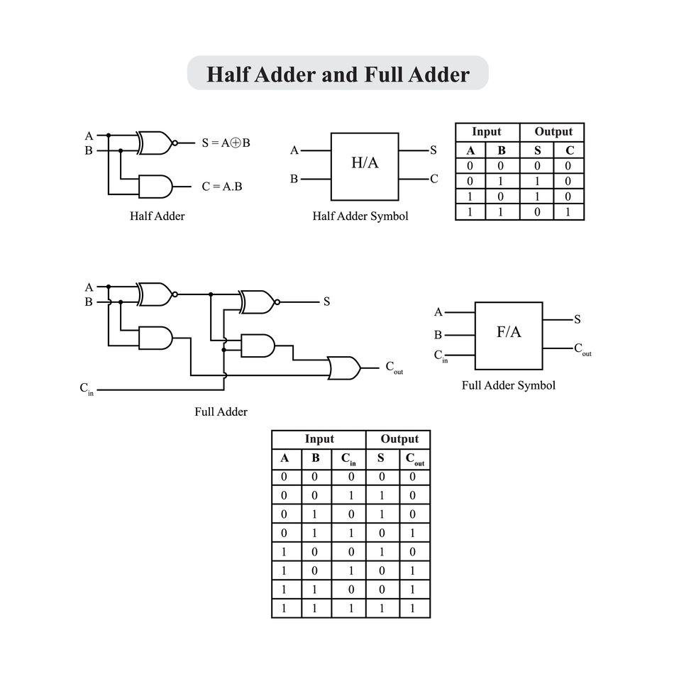
However, if a carry arrives from a previous stage, the half adder cannot process it.
A full adder solves this problem by accepting an additional carry-in bit. This allows it to add three bits—two operands and a carry—and produce a sum and carry-out, making it suitable for cascading in multi-bit adders.
Feature | Half adder | Full adder |
Inputs | A, B | A, B, Carry-in |
Carry handling | None | |
Outputs | Sum and carry | Sum and carry-out |
Complexity | Simple | |
Typical use | Building block of full adders | Multi-bit addition, digital processors |
Recommended Reading: Half Adder Circuit—Theory, Design, and Implementation
Logic description of a full adder
A full adder is a combinational circuit that adds two binary digits and a carry bit and generates a sum bit and a carry bit. Internally, one XOR gate, three AND gates, and one OR gate connect to realise the circuit. The operation is straightforward:
Inputs: A, B and Cin
Sum output (S): A ⊕ B ⊕ Cin
Carry output (Cout): A·B + A·Cin + B·Cin
The truth table for the full adder, reproduced below, shows all eight input combinations and their corresponding outputs:
A | B | C_in | Sum | C_out |
0 | 0 | 0 | 0 | 0 |
0 | 0 | 1 | 1 | 0 |
0 | 1 | 0 | 1 | 0 |
0 | 1 | 1 | 0 | 1 |
1 | 0 | 0 | 1 | 0 |
1 | 0 | 1 | 0 | 1 |
1 | 1 | 0 | 0 | 1 |
1 | 1 | 1 | 1 | 1 |
We can summarize the truth table with the following Boolean expressions:
S=A⊕B⊕Cin
Cout=AB+ACin+BCin
Using these expressions, designers can derive logic gate implementations or optimise the circuit using Karnaugh maps and Boolean algebra.
Implementing a Full Adder
Using half adders and basic gates
One intuitive way to build a full adder is to combine two half adders with an OR gate. When two half adder circuits are connected, the first adds inputs A and B, and its sum is fed into a second half adder along with the carry-in.
The two carry outputs from these half adders are ORed to produce the final carry. This modular approach explains the relationship between half and full adders but also simplifies testing and debugging when designing in hardware description languages (HDLs).
When implementing this structure with logic gates, each half adder uses an XOR gate for the sum and an AND gate for the carry. The resulting full adder consists of two XOR gates, two AND gates and one OR gate.
Universal gate implementations
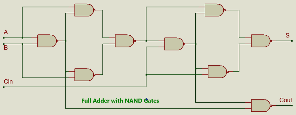
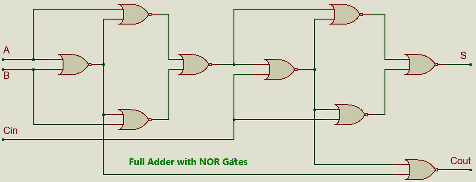
Many teaching labs require building circuits from universal gates to demonstrate gate equivalence. A full adder can be implemented using only NAND gates or only NOR gates.
A NAND‑only design utilises nine NAND gates. It features two half adder equivalents and an extra NAND to combine carries.
A NOR‑only design is the same as the NAND implementation, but designed with NOR gates.
CMOS and Transistor-level Designs
At the integrated circuit level, designers translate the logic functions into transistor networks. Conventional CMOS full adders use complementary pull-up and pull-down networks.
With 28 transistors, a typical 1.8 V CMOS full adder dissipates between 1084 and 1217 nW and has a propagation delay of approximately 22–32 ps. To reduce power and area, researchers explore alternative logic styles such as:
Gate Diffusion Input (GDI) - GDI techniques build logic gates using fewer transistors. Studies suggest that GDI‑based full adders can achieve up to 14.8% power savings and 55% area reduction in a 4-bit adder compared with standard CMOS designs. They can also improve delay and energy consumption by over 41% and 32% respectively.
Hybrid GDI–multi-threshold (MVT) architectures - Combining GDI with multi-threshold transistors further improves energy efficiency, providing more than 57% energy savings and a 92% reduction in energy‑delay product.
Pass-transistor logic and transmission gates - Alternative logic styles reduce transistor count by allowing transistors to act as switches that pass signals rather than generating them. Designs such as 14-transistor or 10-transistor full adders deliver full output voltage swing while saving area and power.
When selecting a transistor-level implementation, engineers must consider fabrication process constraints. GDI and hybrid logic often require twin-well or silicon-on-insulator (SOI) processes, which may be unavailable in standard CMOS processes.
Suggested Reading: Fully Depleted Silicon on Insulator (FDSOI) Theory, Design and Applications for Modern Engineers
Multi-bit Adder Architectures
A single full adder handles one bit. To add multi-bit numbers, designers cascade full adders, connecting the carry-out of the less significant stage to the carry-in of the next stage.
Ripple Carry Adder
Connecting ‘n’ full adders in series yields an n‑bit ripple carry adder. The cascaded design creates a ripple carry adder where the carry-out of each stage becomes the carry-in of the next. The carry signal “ripples” through all stages from the least significant bit (LSB) to the most significant bit (MSB), giving the architecture its name.
Because each stage must wait for the previous stage to compute its carry, the total propagation delay grows linearly with the number of bits.
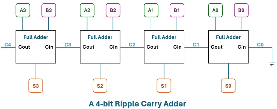
For example, if each full adder has a 20 ns delay, the most significant sum bit in a 4-bit ripple carry adder becomes valid after about 60 ns because the carry must traverse three stages.
Ripple carry adders are suitable for low-cost microcontrollers, small ALUs, or teaching purposes where speed is less critical. However, high-performance processors require faster adder architectures.
Carry Look-ahead Adder
A carry look-ahead adder (CLA) improves speed by computing carry bits in parallel rather than waiting for them to propagate. It generates propagate (P) and generate (G) signals for each bit: a generate signal means the bit will create a carry regardless of the incoming carry, whereas a propagate signal indicates that a carry will be passed through.
Using these signals, the circuit derives carry bits for all stages concurrently. The resulting sum bits are then computed using the previously calculated carries.
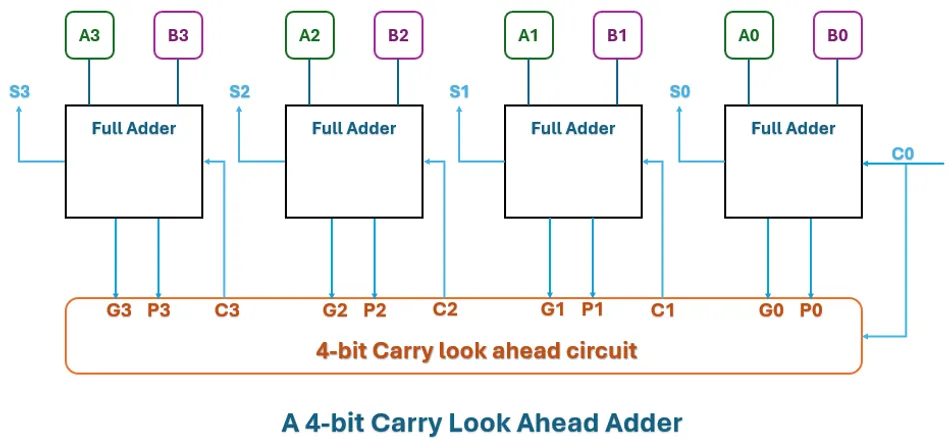
Parallel computation dramatically reduces the overall delay. However, CLAs require extra logic to compute P and G signals and combine them, increasing gate count, power consumption and silicon area.
Other Adder Architectures
Beyond ripple carry and CLAs, engineers employ various architectures to optimise different metrics:
Carry-select adders - The inputs are partitioned into segments. Each segment precomputes two sums—assuming the incoming carry is 0 and assuming it is 1.
Carry-skip (carry-bypass) adders - If certain bits do not generate a carry, the incoming carry can bypass them, reducing delay.
Parallel prefix adders such as Kogge–Stone and Brent–Kung - These use tree structures to compute carries in logarithmic time, offering high performance at the cost of complex wiring.
Emerging technologies. Research explores quantum-dot cellular automata, memristor-based adders, and other non-CMOS devices as potential future solutions.
Recommended Reading: Comprehensive Guide to 4-bit Adders: Theory, Implementation and Modern Innovations
Practical Implementation Using Standard ICs
While modern processors integrate 32- or 64-bit adders into their arithmetic logic units, discrete 4-bit full adder chips remain valuable in education and prototyping.
The 74LS83 (TTL) and 74HC83 (CMOS) are classic 4-bit adder ICs that implement carry look-ahead logic. According to Wevolver, these chips add two 4-bit numbers A0–A3 and B0–B3, accept a carry-in and output four sum bits and a carry-out.
The CMOS variant (74HC83) operates from 2 V to 6 V and sources up to ±4 mA, making it suitable for low-power applications, whereas the TTL variant (74LS83) requires 5 V and offers higher current sink capability.
When building a circuit with these ICs, follow these steps:
Power supply: Provide a stable 5 V supply for TTL devices or 2–6 V for CMOS devices. Use decoupling capacitors across the power pins to suppress noise.
Input connections: Use DIP switches, microcontroller pins or logic generators to drive inputs. Tie unused inputs to a defined logic level (0 or 1) to avoid floating nodes.
Carry handling: If cascading two ICs to create an 8-bit adder, connect the carry-out of the lower nibble to the carry-in of the higher nibble. Many 4-bit adder chips include fast carry pins to simplify this connection.
Output indication: Connect LEDs or a logic analyzer to the sum outputs to observe results. Always include appropriate series resistors when driving LEDs.
Testing: To verify correctness, apply exhaustive input combinations. A 4-bit adder with a carry-in has 512 possible combinations, though selected test vectors can cover typical scenarios.
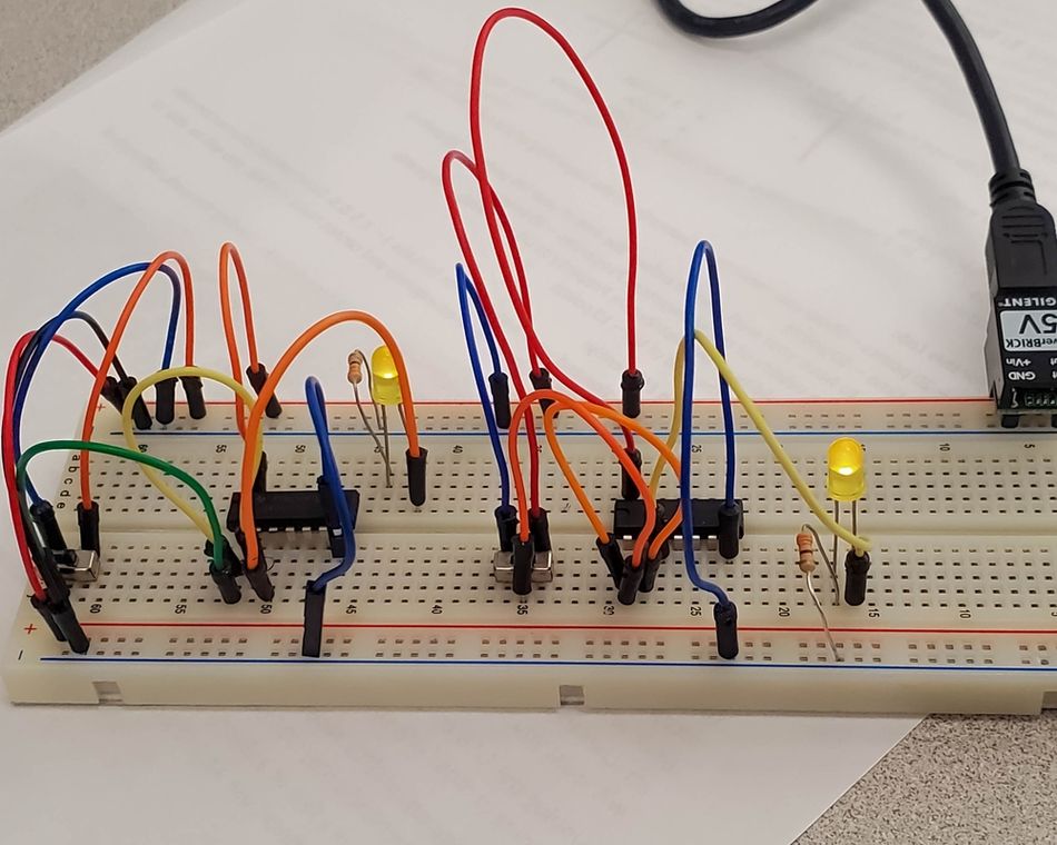
These off-the-shelf devices provide a convenient starting point for students to experiment with binary addition and for engineers to prototype larger designs before integrating them into FPGAs or ASICs.
Suggested Reading: FPGA Design: A Comprehensive Guide to Mastering Field-Programmable Gate Arrays
HDL design flow and simulation
In professional settings, full adder circuits are described in hardware description languages (HDLs) such as Verilog or VHDL. Wevolver outlines a typical design flow for a 4-bit adder, which applies equally to a single full adder:
Module definition: Write HDL modules for half adder and full adder, clearly specifying inputs (A, B, Cin) and outputs (Sum, Cout).
Instantiation: Create a top-level module that instantiates the required number of full adders. Connect inputs and route carries appropriately. For a CLA, implement the propagate and generate logic.
Simulation: Develop a testbench that applies various input vectors. Use simulation tools to verify that the outputs match the expected truth table across all combinations.
Synthesis: Translate the HDL into a gate-level netlist. Use synthesis tools to map the design to the target FPGA or ASIC technology. Analyse timing to ensure the design meets performance targets.
Implementation: Place and route the design, load the configuration onto hardware, and perform hardware verification. Adjust constraints and design choices as needed to meet power and area goals.
Recommended Reading: Guide to Mastering SystemVerilog: Elevate Your Hardware Design and Verification Skills
Advantages, Applications and Design Considerations
Benefits of full adder circuits
Compared with a half adder, the full adder offers several advantages. It can handle incoming carries, produces higher output and consume relatively less power in comparison to multiple half adders working together.
The ability to be converted into a half subtractor by adding a NOT gate adds versatility. Full adders are also essential building blocks in more complex digital circuits such as multiplexers and ALUs, performing additions at higher speed.
Practical applications
Full adder circuits appear throughout digital hardware:
ALUs and CPUs -Full adders form the core of arithmetic logic units in processors. They add binary numbers, compute addresses and support arithmetic instructions like increment and addition. Without them, modern computing would not be possible.
Calculators and Embedded Systems - Many consumer devices, from calculators to digital watches, include full adder circuits to perform arithmetic.
Multipliers and address generators - Multiplication can be implemented via repeated addition, so arrays of full adders accumulate partial products. Address generation in memory controllers also relies on adders.
Graphics processing units (GPUs) - Full adders are used in fixed-point and floating-point units to compute pixel values, vertex coordinates and other graphics operations.
Communication systems and error detection - Adders contribute to cyclic redundancy check (CRC) algorithms and parity generation.
Design Considerations for Full Adders
When designing or selecting a full adder circuit for a project, engineers should evaluate several factors:
Power consumption - Mobile devices and Internet-of-Things nodes demand low power. GDI and hybrid logic provide significant energy savings. Lowering supply voltage and using multi-threshold transistors also reduce power.
Propagation delay = High-performance processors cannot tolerate long delays. Carry look-ahead, carry-select and parallel prefix adders reduce delay at the cost of more hardware.
Area - A Compact area lowers cost and allows more functions on a chip. Ripple carry adders minimise gate count but suffer from speed limitations. GDI reduces transistor count for small designs.
Noise margins and voltage swing - Certain logic styles (e.g., pass-transistor logic) may degrade signal swing. Designers must ensure outputs remain within logical thresholds.
Technology and fabrication constraints - Some advanced techniques require special fabrication processes (SOI or twin-well), which may not be available in all manufacturing nodes.
Scalability - For large word lengths, advanced adder architectures like parallel prefix adders may be necessary to maintain performance.
Conclusion
The full adder circuit is more than a simple logic block; it is the foundation of digital arithmetic. Understanding how it works, how to build it with basic gates or universal gates, and how to cascade it into multi-bit adders is essential for any engineer working in digital electronics. Ripple carry adders demonstrate the simplicity of cascading full adders but reveal the limitation of linear propagation delay. Carry look-ahead and other architectures mitigate this delay by computing carries in parallel, trading complexity for speed. Modern research continues to push the boundaries with energy-efficient designs using techniques like GDI and hybrid logic, delivering significant power and area savings.
Off-the-shelf ICs and HDL implementations provide practical avenues for learning and prototyping, while advanced architectures support the demands of high-performance computing. By mastering the theory and practice of full adder circuits, engineers can design more efficient and reliable arithmetic units, optimise power and speed, and contribute to innovations in digital hardware. As technology scales and new devices emerge, the humble full adder remains a central component of computational logic, evolving through research and engineering ingenuity.
FAQs
1. What is a full adder circuit?
A full adder circuit is a combinational logic network that adds three binary inputs—two operands and a carry-in—and outputs a sum and carry. It differs from a half adder by handling an incoming carry bit.
2. How is a full adder implemented using half adders?
Two half adders are connected in series: the first half adder adds the operand bits, and its sum is fed into a second half adder along with the carry-in. The carry outputs of the two half adders are ORed to produce the final carry.
3. What is the difference between ripple carry and carry look-ahead adders?
Ripple carry adders cascade full adders so that the carry ripples from the least significant bit to the most significant bit, leading to linear delay with bit width. Carry look-ahead adders compute carries in parallel using propagate and generate signals, reducing delay but increasing hardware complexity.
4. Why are Gate Diffusion Input (GDI) techniques used in full adder design?
GDI techniques implement logic functions using fewer transistors than standard CMOS. Research shows that GDI\‑based full adders save approximately 14.8 % in power and 55 % in area while improving delay and energy metrics.
5. What are the typical applications of full adder circuits?
Full adders are central to arithmetic logic units in CPUs and ALUs, calculators, digital signal processors, multipliers, address generators and graphics processing units. They also support functions like error detection and correction.
6. Can a full adder be realised using only NAND or NOR gates?
Yes. Since NAND and NOR gates are universal, a full adder can be implemented using nine NAND gates or a corresponding network of NOR gates. These implementations are useful for educational purposes and for processes where NAND or NOR logic is preferred.
7. Are there other adder architectures beyond ripple carry and carry look-ahead?
Yes. Engineers use architectures such as carry-select, carry-skip, and parallel-prefix (e.g., Kogge–Stone) adders to trade off speed, area, and complexity. Emerging research explores quantum-dot cellular automata and memristor-based adders for future technologies.
References
C. “Circuit Digest.” CircuitDigest.com. [Online]. Available: https://circuitdigest.com.
“Tutorials Point.” TutorialsPoint.com. [Online]. Available: https://www.tutorialspoint.com.
Abhishek Sharma, Gati Goyal, Nikunj Agarwal, Ayush Jain, “16 Bit Carry Skip Adders.” [Online]. Available: https://www.fpga-systems.ru/library/_unsorted/carry_skip_adders.pdf
in this article
1. Key takeaways2. Introduction3. Binary Addition - Why Do We Need a Full Adder?4. Implementing a Full Adder5. Multi-bit Adder Architectures6. Practical Implementation Using Standard ICs7. HDL design flow and simulation8. Advantages, Applications and Design Considerations9. Conclusion10. FAQs11. References