Featured
NVIDIA TAO and Edge Impulse integrate to streamline the development and deployment of edge AI models, empowering developers to quickly build and optimize AI applications for diverse hardware environments.
NVIDIA TAO and Edge Impulse integrate to streamline the development and deployment of edge AI models, empowering developers to quickly build and optimize AI applications for diverse hardware environments.
PCB Trace Width Calculator
Glossary of Semiconductors Terms
NVIDIA TAO and Edge Impulse integrate to streamline the development and deployment of edge AI models, empowering developers to quickly build and optimize AI applications for diverse hardware environments.
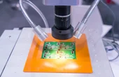
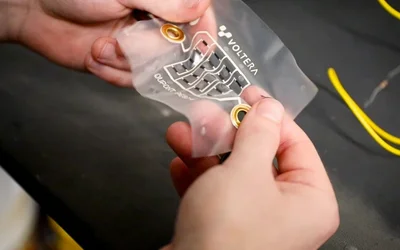
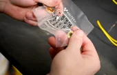
Researchers at MIT used a Voltera NOVA to successfully print field electron emitters with a high-concentration carbon nanotube ink. The research has exciting implications for small satellites.
Unlock the secrets to enhancing electronic system performance through strategic PCB stackup configurations, crucial for ensuring signal integrity and mechanical stability.
Semiconductors are the building blocks of modern electronics, powering everything from smartphones to satellites. This in-depth guide provides a comprehensive understanding of semiconductors' engineering principles and applications, delving into their fundamental concepts, materials, devices, manufacturing processes, and their impact on today's technology landscape.
13 minutes read.
20 minutes read.
16 minutes read.
20 minutes read.
20 minutes read.
13 minutes read.


Semiconductors
Nordic Semiconductor is a fabless semiconductor company specializing in wireless technology that powers the IoT.
181 Posts
A guide covering the full radio-frequency design workflow, starting from setting specifications and choosing topologies to matching, simulation, layout, and verification, to help antenna engineers.
This article presents a detailed technical exploration of SiC MOSFET devices, covering material physics, device structure, switching behavior, and practical design considerations for high-efficiency power electronics systems.
This article is a comprehensive technical guide to relay wiring diagrams, covering 4-pin and 5-pin configurations, working principles, safety practices, standards, and advanced relay applications in modern systems.
Explore how frequency shapes EMC behavior from RF emissions to ultra-low-frequency drift, with mitigation strategies for robust, compliant electronic system design.
How Essentra Components Supports Engineering from Concept to Production
Makera gives live demonstrations of the Z1 during the 2026 Hackaday Europe event. The Z1 is a compact CNC manufacturing platform.
A crystal oscillator is an electronic circuit that uses a quartz crystal to produce a precise and stable frequency reference. This article covers crystal operation, equivalent circuit models, resonance, load capacitance, oscillator topologies, stability, aging, and design practices.
June 25, 2026 at 08:00 PM Central European Summer Time
NVIDIA TAO and Edge Impulse integrate to streamline the development and deployment of edge AI models, empowering developers to quickly build and optimize AI applications for diverse hardware environments.
Researchers at MIT used a Voltera NOVA to successfully print field electron emitters with a high-concentration carbon nanotube ink. The research has exciting implications for small satellites.
Unlock the secrets to enhancing electronic system performance through strategic PCB stackup configurations, crucial for ensuring signal integrity and mechanical stability.
PCBs printed onto flexible substrates demonstrate huge potential across a range of industries. But what are the materials used to make these printed devices?
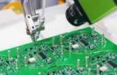
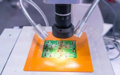
The miniaturization of electronics is widely attributed to advances in semiconductor technology as observed by Moore’s Law, but many overlook the design and manufacturing challenges involved in utilizing small device packages such as ball grid arrays.

5 minutes read
A comprehensive exploration of open circuits, detailing their characteristics, detection methods, and the pivotal role they play in modern engineering systems.
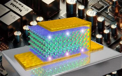
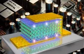
Sang-Hoon Bae developed heterostructures with material properties optimal for high-density energy storage, durable ultrafast charging

3 minutes read
This article delves into the innovative world of flexible printed circuit boards, uncovering their design, advancements, and transformative role in modern engineering applications.
UAV technology continues to expand and become increasingly sophisticated.

4 minutes read
Wire Electrical Discharge Machining (Wire EDM) has revolutionized precision machining, empowering manufacturers to tackle with intricacies in aerospace, medical devices, and electronics. This latest technology pushes boundaries with its ability to create complex shapes and achieve point accuracy.
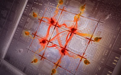
The advance offers a way to characterize a fundamental resource needed for quantum computing.
Exploring the Trends, Challenges, and Innovations Shaping the Future of Engineering. Complete the survey to enter the prize draw!
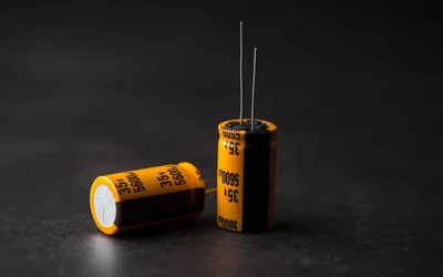
This guide explores the crucial factors in capacitor polarity, its mathematical analysis, identification, and advanced practices for improved circuit performance.
Explore the different types of solder, their unique properties, and their critical roles in various engineering applications. Understand how to choose the right solder for your project and the considerations involved.
Autonomous robotics must anticipate and plan for the unexpected, often in harsh, changing environments. We take a deep dive into these challenges by exploring design considerations beyond those associated with conventional PCBAs.
6 minutes read