What are Circuit Boards Made Of? An Extensive Guide to Materials and Manufacturing Processes
Unveiling the Art and Science Behind Circuit Boards - Copper Etching to Silkscreens, a Comprehensive Guide to Elements, Manufacturing Processes, and Multilayered Varieties in Electronic Circuit Boards

21 Nov, 2023. 14 minutes read
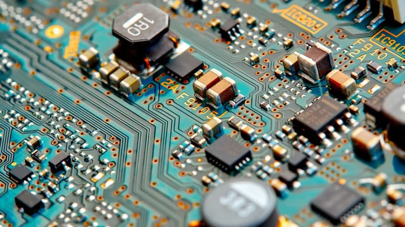
A circuit board showing its traces, vias, electronic components, solder mask and more.
What are Circuit Boards?
Circuit boards, also known as printed circuit boards (PCBs), are the backbone of virtually all modern electronic devices. From smartphones and computers to advanced medical equipment and electric vehicles, circuit boards play a crucial role in the functionality of these devices. They are perhaps the most critical part of modern electrical and electronic systems.
A circuit board is a physical piece of technology that allows for the creation of complex electronic circuits. It’s the foundation upon which electronic components such as resistors, capacitors, and integrated circuits (ICs) are mounted and electrically connected. The board is typically made from a flat, rigid, non-conductive material or substrate, often fibreglass or plastic, to ensure proper performance. They allow for high functionality and complexity to be packed into a small, manageable form factor., empowering miniaturization of electronics, and leading to the development of compact, portable devices.
Further Reading: How Do Circuit Boards Work: A Comprehensive Guide to the Heart of Electronics
Basic Components of a Circuit Board
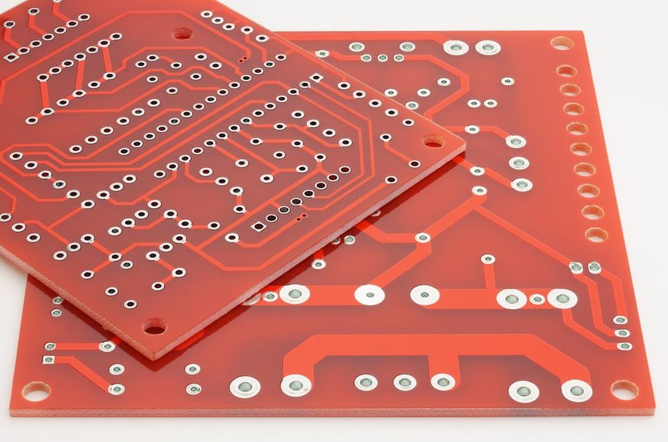
A circuit board comprises several key components, each serving a specific function in the overall operation of the electronic device. These components include conductive pathways, substrate material, solder mask, and silkscreen.
Conductive Pathways
Conductive pathways, often called traces, are thin lines of conductive material, typically copper, that are etched onto the surface of the circuit board. These are highly conductive tracks etched on the circuit board to serve as wiring, allowing electrical signals to travel between the various components mounted on the board.
A circuit board consists of a copper layer with a fixed thickness. Depending on the current carrying requirements, the trace width is the only parameter designers can control. Hence, wider traces are used for higher current paths.
Generally, the thickness of the copper layer used to create these pathways is typically measured in ounces per square foot, with a standard thickness of 1 ounce of copper per square foot of the board, equating to a thickness of approximately 1.37 mils (thousandths of an inch) or 35 micrometers. In designer slang, it’s referred to as 1oz Copper. The following table shows copper thickness in commonly preferred units:
1 | oz |
1.37 | mils |
0.00137 | inch |
0.0347 | mm |
34.79 | µm (micron/micrometer) |
Copper is the material of choice for these pathways due to its excellent electrical conductivity, which is surpassed only by silver. It’s also relatively easy to etch, making it suitable for the manufacturing process of circuit boards.
However, since bare copper is prone to oxidation, it can degrade its conductivity over time. Therefore, copper traces are usually coated with a thin layer of solder, gold, or a nickel-gold alloy, which protects the copper from oxidation while providing a solderable surface for mounting electronic components.
Substrate Material
The substrate, often referred to as the base material, is the solid, non-conductive foundation upon which the other components of a circuit board are built. It provides mechanical strength to the board and acts as an electrical insulator between the layers of conductive material.
The most commonly used substrate for circuit boards is a glass-reinforced epoxy laminate known as FR-4 (Flame Retardant type 4). This material is chosen for its desirable properties:
Good strength-to-weight ratio
Low cost
Excellent electrical insulation.
The "FR" in FR-4 indicates that the material is flame retardant, a critical safety feature for electronic devices.
These materials can be used for circuits for up to 7GHz. The preferred substrate materials for higher frequencies are Polyamide, Ceramics, and Metal-core substrates.
Polyimide is often used in flexible circuit boards due to its excellent flexibility and heat resistance.
Ceramic substrates are used in high-frequency and high-power applications due to their superior electrical and thermal properties.
Metal-core substrates typically consist of an aluminum core with a non-conductive dielectric layer. They are used in LED lighting applications for their excellent heat dissipation capabilities.

PCB substrate specifications play a pivotal role in their selection. Typically, the substrate is chosen according to the following physical specs.
Thickness and Rigidity - The thicker the substrate, the less it will bend. The standard thickness is 1.57 mm, but there are thinner and thicker options available.
Glass Transition Temperature (Tg) - The temperature at which the epoxy impregnated in the fibreglass starts to soften. Higher Tg is essential for high-power circuits as they generate more heat.
Di Electric Constant (Dk) - It measures how well the electric lines of force will travel through the substrate material.
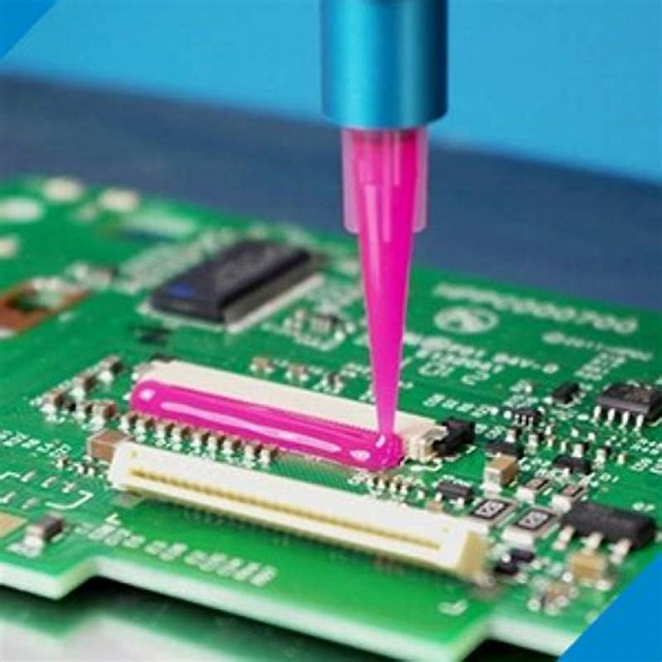
Solder Mask
The solder mask is a critical circuit board component that serves multiple functions. It is a thin layer of polymer material that is applied over the copper traces and vias of the circuit board, leaving only the areas to be soldered exposed. This layer is typically green but can also be in other colors, such as blue, red, or black.
Primarily, the solder mask prevents the formation of solder bridges between closely spaced solder pads during the soldering process. Solder bridges can create short circuits, which can cause the electronic device to malfunction or even fail. Therefore, covering the copper traces and vias with a solder mask ensures that the solder flows only onto the exposed solder pads and not onto the traces.
Image Source: Solder Mask in PCB Manufacture Process

The solder mask also protects the copper traces from environmental factors such as moisture and dust, which can cause corrosion and degradation of the copper over time. It further provides electrical insulation, helping prevent short circuits between adjacent traces.
The solder mask is typically applied using a process known as screen printing, where the solder mask material is forced through a stencil or screen that has openings where the solder pads are located.
Recommended Reading: Via Tenting for PCBA Design
Silkscreen
The silkscreen provides important information about the board and its components. It is a layer of ink printed onto the circuit board's surface, typically on top of the solder mask. The silkscreen contains various markings, such as component designators, reference designators, logos, and other text or symbols that aid in the electronic device's assembly, testing, and troubleshooting.
Component designators are labels that identify the type of component, such as "R" for resistors, "C" for capacitors, and "Q" for transistors. Reference designators are unique identifiers assigned to each component on the board, allowing for easy identification and location of specific components during assembly and troubleshooting. For example, a resistor might be labeled "R1," while a capacitor might be labeled "C1."
The silkscreen is typically applied with an epoxy-based, heat-resistant ink, using a screen printing process similar to the solder mask. The ink is long-lasting and can withstand chemicals, moisture to ensure legibility throughout the lifetime of the electronic device. A stencil or screen with the desired pattern is placed over the circuit board, and ink is forced through the openings onto the board's surface.
More advanced techniques, such as inkjet printing and laser marking, have been developed to apply silkscreen. These methods offer higher resolution and greater precision, allowing smaller and more detailed markings to be applied to the circuit board.
Further Reading: Silkscreen on a PCB: What is it?
The Manufacturing Process of Circuit Boards
The manufacturing process of circuit boards is a complex, multi-step procedure involving various techniques and technologies.
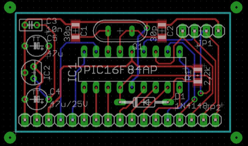
Designing the Circuit Board
The first step in the manufacturing process is designing the circuit board, which is typically done using Computer-Aided Design (CAD) software. It allows engineers to create a detailed, digital representation of the circuit board.
The design includes the layout of the components, the routing of the conductive pathways, and the placement of the holes for mounting components and creating electrical connections between different layers of the board.
The design process begins with creating a schematic diagram, a symbolic representation of the electronic circuit. The schematic shows all the circuit components and how they are connected. The schematic is converted into a layout, a physical representation of the circuit board. The layout shows the board's exact size and shape, the components' location, and the routing of the conductive pathways.
Image Source: The Line Grinder Help: Configuring Eagle
The layout is then checked for errors using a process known as Design Rule Check (DRC). The DRC checks for potential issues such as traces that are too close together, components that are too close to the edge of the board, and holes that are too close to traces or other holes. If any errors are found, the layout is adjusted, and the DRC is run again until no errors are found.
Once the layout is finalised, it is converted into a set of manufacturing files known as Gerber files. These files contain all the information needed to manufacture the circuit board, including the size and shape of the board, the location and size of the holes, the layout of the traces, and the placement of the components. The Gerber files are then sent to the circuit board manufacturer, who uses them to create the physical circuit board.
Further Reading: How to Design a PCB Layout: A Comprehensive Guide
Creating the Substrate
The substrate provides the mechanical support for the circuit and acts as an electrical insulator between the conductive layers. The most common material used for the substrate is FR-4, a type of glass-reinforced epoxy laminate. The process of creating the substrate begins with preparing the fibreglass cloth. The cloth is cut to the desired size and then impregnated with the epoxy resin.
This is typically done using a process known as prepreg-ging, where the fibreglass cloth is dipped into a bath of the epoxy resin and then passed through heated rollers to remove excess resin and ensure a uniform thickness.
The fibreglass is then layered together with copper foil sheets. The number of layers can vary depending on the complexity of the circuit board, with more complex boards requiring more layers. The layered materials are then placed into a press, where they are subjected to heat and pressure. This causes the epoxy resin to flow and then cure, bonding the layers together and forming a rigid board.
The substrate thickness can vary depending on the requirements of the circuit board. Common thicknesses range from 0.031 inches (0.79 mm) to 0.125 inches (3.18 mm). The thickness is controlled by the number of layers of fibreglass cloth used and the thickness of each layer.
Recommended Reading: PCBs Thickness: Understanding Thickness Variations
Adding the Copper Layer
The copper layer forms the conductive pathways, electrically connecting the PCB components together. It’s pivotal in the circuit board manufacturing process.
A thin copper foil layer is applied to both sides of the substrate by using a lamination process. The copper foil and the substrate are passed through heated rollers that apply pressure, causing the copper to bond to the substrate.
After copper foil lamination, the circuit pattern is created via imaging. Here, the board is coated with a layer of photoresist, a light-sensitive material, and then exposed to ultraviolet light through a mask containing the circuit pattern. The areas of the photoresist that are exposed to the light harden, while the unexposed areas remain soft.
Later, the unhardened photoresist is removed, revealing the underlying copper. The board is then etched, removing the exposed copper and leaving behind the copper under the hardened photoresist. This forms the circuit pattern.
The remaining photoresist is stripped away, leaving behind the copper circuit pattern. Next, the board is cleaned to remove any remaining photoresist or etchant residue. The result is a circuit board with a copper layer that forms the conductive pathways of the circuit.
Applying the Solder Mask
Solder mask application begins with the preparation of the solder mask material. This material is typically a type of epoxy resin that is mixed with a hardener and a pigment, which gives the solder mask its characteristic color, most commonly green.
The solder mask material is then applied to the circuit board using a process known as screen printing. In this process, a stencil or screen with the desired pattern is placed over the circuit board, and the solder mask material is forced through the openings in the screen onto the board's surface. The thickness of the solder mask layer is typically around 0.025 mm, but can vary depending on the requirements of the circuit board.
Image Source: gabrielleelmore | Dual Monitor Background
Once the solder mask material is applied, the board is subjected to a curing process. This typically involves baking the board in an oven at a temperature of around 150°C for approximately one hour. This causes the solder mask material to harden and adhere to the board's surface.
The board is then inspected to ensure that the solder mask has been correctly applied and that all the necessary areas have been left exposed for soldering. Any necessary corrections are made at this stage before the board proceeds to the next step in the manufacturing process, which is the application of the silkscreen.
Adding the Silkscreen
This is the final step in the manufacturing process of a circuit board is the silkscreen application. A stencil or screen with the desired pattern is placed over the circuit board, and ink is forced through the openings onto the board's surface.
Once the silkscreen ink is applied, the board is subjected to a curing process, which typically involves baking the board in an oven at around 150°C for approximately one hour. This causes the ink to harden and adhere to the board's surface.
The circuit board undergoes an inspection to ensure the markings are clear and accurate. Any necessary corrections are made before the board is shipped to the assembler for component mounting and soldering.
Types of Circuit Boards
Circuit boards can be classified into several types based on their design and construction. These types include single-sided boards, double-sided boards, and multi-layer boards.
Single-Sided Boards
Single-sided boards are the simplest and most basic type of circuit board. As the name suggests, these boards have conductive pathways on only one side of the substrate, making them relatively easy and inexpensive to manufacture, as there is no need for complex processes to create connections between multiple layers.
Single-sided boards are typically used in low-cost, low-complexity electronic devices, such as simple consumer electronics, toys, and basic control systems.
Due to their simplicity, single-sided boards have some limitations regarding routing density and component placement. This means that they are unsuitable for more complex electronic devices requiring a higher level of integration and functionality.
Double-Sided Boards
Double-sided boards are a step up in complexity from single-sided boards. These boards have conductive pathways on both sides of the substrate, which allows for a higher density of components and a more complex circuit design.
The key feature of double-sided boards is through holes or vias to connect the conductive pathways on one side of the board to those on the other. Drilling holes in the substrate creates these through-holes and then plating them with copper to create a conductive path. The use of through-holes increases the complexity of the manufacturing process, but it also provides greater flexibility in terms of component placement and circuit design.
Double-sided boards are commonly used in various electronic devices, including computers, telecommunications equipment, and industrial control systems. They balance complexity and cost well, making them a popular choice for many applications.
Multi-Layer Boards
Multi-layer boards represent the pinnacle of complexity in circuit board design. These boards consist of multiple layers of conductive pathways, separated by insulating substrate layers. The number of layers can range from four to over thirty, although four to twelve layers are most common in general applications.
The primary advantage of multi-layer boards is their high density of interconnections. This allows for complex, high-speed circuit designs that are not feasible with single-sided or double-sided boards. These are typically used in high-performance electronic devices such as computers, servers, and telecommunications equipment, where high speed, high capacity, and compact size are critical.
Image Source: https://circuits-diy.com/how-to-make-a-multilayer-pcb-at-home-a-beginners-guide/
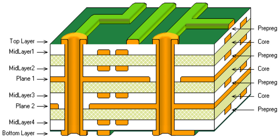
The manufacturing process for multi-layer boards is significantly more complex than for single-sided or double-sided boards. Each layer of copper and substrate is created separately, and the circuit pattern is etched onto each copper layer. The layers are then stacked together and bonded under heat and pressure in a process known as lamination. After lamination, the board is drilled and plated to create through holes and vias that connect the different layers.
One of the key challenges in designing and manufacturing multi-layer boards is managing the electrical properties of the board. As the number of layers increases, issues such as signal integrity, impedance control, and thermal management become increasingly important. These issues require careful design and precise control of the manufacturing process to ensure that the finished board performs as intended.
Further Reading: What is a Multilayer PCB? (wevolver.com)
Conclusion
Circuit boards are a fundamental component of virtually all electronic devices, and their design and manufacturing process is complex and intricate. Each step requires precision and expertise, from the initial design phase to the final application of the silkscreen. The type of circuit board, whether a single-sided, double-sided, or multi-layer board, also plays a significant role in determining the complexity of the manufacturing process.
The evolution of circuit board technology has been driven by the increasing demand for smaller, more powerful electronic devices. As these trends continue, the complexity of circuit board design and manufacturing is likely to increase, with a greater emphasis on multi-layer boards and advanced manufacturing techniques.
Frequently Asked Questions
1. What is a circuit board?
A circuit board is a thin board made of an insulating material onto which conductive pathways are printed or etched. These pathways connect various electronic components, allowing them to work together to perform complex functions.
2. What are the different types of circuit boards?
Circuit boards can be classified into several types based on their design and construction. These include single-sided boards, which have conductive pathways on only one side of the board; double-sided boards, which have pathways on both sides; and multi-layer boards, which have multiple layers of conductive pathways separated by insulating layers.
3. What is the purpose of the solder mask on a circuit board?
The solder mask is a protective layer that covers most of the circuit board's surface, leaving only the areas that will be soldered exposed. It serves several important functions, including preventing solder bridges, protecting the copper traces from environmental damage, and providing electrical insulation.
4. What is the silkscreen on a circuit board?
The silkscreen is a layer of ink that contains important information about the board and its components. This can include component designators, reference designators, logos, and other text or symbols that aid in assembly, testing, and troubleshooting.
5. What are through-holes and vias on a circuit board?
Through-holes and vias are used on double-sided and multi-layer boards to connect the conductive pathways on one side to those on the other. Drilling holes in the substrate create them and then plating them with copper to create a conductive path.
References
in this article
1. What are Circuit Boards?2. Basic Components of a Circuit Board3. The Manufacturing Process of Circuit Boards4. <span class="fr-mk" style="display: none;"> </span><span class="fr-mk" style="display: none;"> </span><span class="fr-mk" style="display: none;"> </span><span class="fr-mk" style="display: none;"> </span><span class="fr-mk" style="display: none;"> </span><span class="fr-mk" style="display: none;"> </span><span class="fr-mk" style="display: none;"> </span><span class="fr-mk" style="display: none;"> </span><span class="fr-mk" style="display: none;"> </span><span class="fr-mk" style="display: none;"> </span><span class="fr-mk" style="display: none;"> </span><span class="fr-mk" style="display: none;"> </span><span class="fr-mk" style="display: none;"> </span><span class="fr-mk" style="display: none;"> </span><span class="fr-mk" style="display: none;"> </span><span class="fr-mk" style="display: none;"> </span><span class="fr-mk" style="display: none;"> </span><span class="fr-mk" style="display: none;"> </span><span class="fr-mk" style="display: none;"> </span><span class="fr-mk" style="display: none;"> </span><span class="fr-mk" style="display: none;"> </span><span class="fr-mk" style="display: none;"> </span><span class="fr-mk" style="display: none;"> </span>5. Types of Circuit Boards6. Conclusion7. Frequently Asked Questions8. References