Featured

Along with ElaadNL, PhD researcher Tim Slangen studied the phenomenon known as supraharmonic disturbances, which can adversely affect the operation and efficiency of electrical appliances.

This guide is written for engineers and technical teams building connected devices who need clear, field-ready guidance without getting lost in standards documentation.
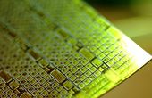
PCB Trace Width Calculator
Along with ElaadNL, PhD researcher Tim Slangen studied the phenomenon known as supraharmonic disturbances, which can adversely affect the operation and efficiency of electrical appliances.
In a world that is increasingly dependent on electronic technology, EMC protection plays a vital role in a wide range of industries. Whether in automotive, aerospace or power generation, EMC protection is essential for the reliability, safety and performance of electronic systems.
In this episode, we talk about how researchers from the Technical University of Denmark are tackling the issue of monoculture farming by utilizing robotics and next-gen image analysis.
Understanding the key differences between the two high-in-demand battery types. This article focuses on Energy density, lifespan, safety, and cost trade-offs for the technical selection of Li-Ion and LiFePO4 batteries.
16 minutes read.
20 minutes read.
15 minutes read.
20 minutes read.
13 minutes read.
28 minutes read.


Electronics
Mouser Electronics is a worldwide leading authorized distributor of semiconductors and electronic components.
219 Posts
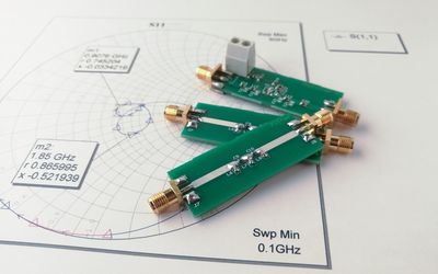
A guide covering the full radio-frequency design workflow, starting from setting specifications and choosing topologies to matching, simulation, layout, and verification, to help antenna engineers.
This article presents a detailed technical exploration of SiC MOSFET devices, covering material physics, device structure, switching behavior, and practical design considerations for high-efficiency power electronics systems.
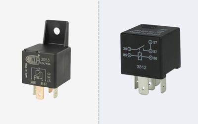
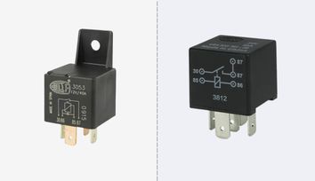
This article is a comprehensive technical guide to relay wiring diagrams, covering 4-pin and 5-pin configurations, working principles, safety practices, standards, and advanced relay applications in modern systems.
Explore how frequency shapes EMC behavior from RF emissions to ultra-low-frequency drift, with mitigation strategies for robust, compliant electronic system design.
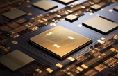
Ultra-efficient chip design enables extremely strong cryptography algorithms to run on energy-constrained edge devices.
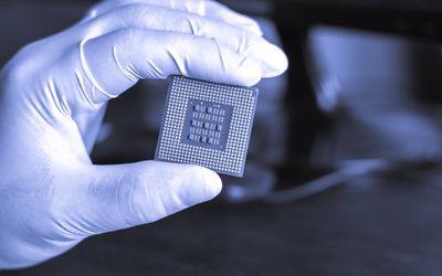
Researchers at ETH Zurich have now developed chip technology that enables verification of the authenticity of sensor data, including images or videos.
The integrated design achieves accurate micro gas chromatography and can help reduce the cost of monitoring chemical synthesis, natural gas pipelines or at-home air quality.
Hybrid bonding provides the adhesive free, copper to copper interconnects that are driving cutting edge 3D chip stacking. This article explains the theory, process, benefits, challenges, applications, and emerging trends of hybrid bonding for engineers.
Along with ElaadNL, PhD researcher Tim Slangen studied the phenomenon known as supraharmonic disturbances, which can adversely affect the operation and efficiency of electrical appliances.

4 minutes read
In a world that is increasingly dependent on electronic technology, EMC protection plays a vital role in a wide range of industries. Whether in automotive, aerospace or power generation, EMC protection is essential for the reliability, safety and performance of electronic systems.

5 minutes read
In this episode, we talk about how researchers from the Technical University of Denmark are tackling the issue of monoculture farming by utilizing robotics and next-gen image analysis.

15 minutes read
In part II of the Mouser podcast episode, Dr. Smit Patel continued discussing the evolving landscape of digital therapeutics and its impact on healthcare highlighting several key insights into how digital solutions are reshaping medical treatments and the regulatory environment surrounding them.
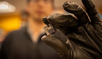
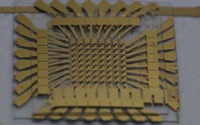
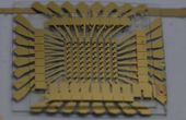
Sang-Hoon Bae and collaborators have demonstrated integrated processing hardware they say could revolutionize AI computing

2 minutes read
This article offers an in-depth view of PVD coating in semiconductors, their underlying technology, materials, and applications crucial in today's rapidly evolving technological landscape.
Volatile Organic Compounds (VOC) sensors are key in detecting potentially dangerous air quality.
Exploring the Fusion of Neuromorphic Computing and Electronic Noses for Advanced Sensory Solutions
Exploring Silicon Photonics: Shaping the Future of Optical Communication
Discover more about the crucial topic of indoor air quality.
In Denmark, agriculture makes up almost 2/3 of our land and oftentimes one crop is grown in huge areas. That's hurting the biodiversity, but agricultural robots can help do away with monoculture, and a new DTU project will pave the way for that future.

5 minutes read
There are times when scientific progress comes in the form of discovering something completely new. Other times, progress boils down to doing something better, faster, or more easily.

4 minutes read
Radio Frequency Identification (commonly known as RFID) is a technology that leverages wireless communication over radio waves to both transfer data and locate objects.

4 minutes read
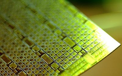
Transistors — the tiny on-off switches inside microchips — have gotten smaller and smaller over the years, increasing computing power and enabling smaller devices. During that time, the copper wires that connect these switches have likewise shrunk.

2 minutes read
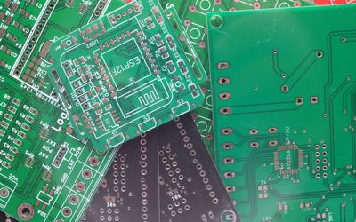
Two primary PCB assembly techniques have emerged as the electronics industry standards: Through-Hole Technology (THT) and Surface Mount Technology (SMT). This article delves into the intricacies of THT and SMT, providing a thorough comparison of their advantages, disadvantages, and applications.