Wafer Thinning: Investigating an essential part of semiconductor fabrication
Wafer thinning is a part of the semiconductor manufacturing process. It is essentially grinding off the backside of the wafers to control their thickness and is useful for the production of ultra-thin wafers. These flattened wafers are used to effect stacked and high-density packaging in compact or microelectronic devices. This article discusses the meaning of wafer thinning, along with its various techniques and significance.

08 Sep, 2022. 4 minutes read
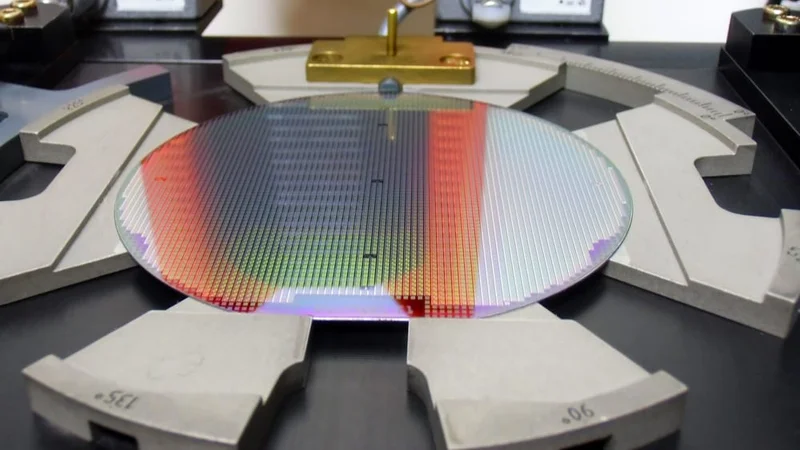
Thin Silicon Wafer
Introduction
Wafer thinning is a stage in semiconductor manufacturing process that aims to reduce wafer thickness. This is so that ultra-thin wafers can be created for more sophisticated integrated circuits (ICs) to meet the evolving electronic market in the production of compact, portable devices.
The wafer thinning process is a complex but essential part of semiconductor manufacturing. It requires highly advanced machines and special environments for the semiconductor wafers to be thinned and then diced into small chips to be used in devices.
What is Wafer Thinning?
Wafer thinning, also known as wafer backgrinding, is a step in the fabrication of semiconductor devices during which wafer thickness is reduced to allow for stacking and high-density packaging of integrated circuits for compact electronic devices.
Wafer thinning is therefore the process of shaving off material from the backside of a wafer until the desired target thickness is finally achieved.[1]
The function of the wafer back grinding process is to grind the substrate material of the wafer, usually silicon, to remove a certain amount of material. It is beneficial to the requirements of the device packaging process, heat dissipation, and size requirements of the chip. Hence the advantages of wafer thinning include:
Reduction of thermal resistance
Improvement of device performance
Improvement of reliability
Lowering overall package height
Reducing die stress, which happens as a result of mismatches in the coefficient of thermal expansion (CTE) between the silicon die and the board materials.[2]
Recommended reading: Silicon Wafers: Everything You Need to Know
Modern electronics continue to usher in portable and lightweight devices such as handheld music players, smartphones, and USB memory sticks. The advent of these would not be possible without minimizing the size of their components. This is what calls for the grinding or thinning of the backside of wafers before wafer dicing (the separation of individual microchips) is done. Wafers are generally about 750 μm thick to ensure mechanical stability and prevent warping during high-temperature processing. However, due to wafer backgrinding, wafers are now commonly thinned down to 75 or 50 μm.
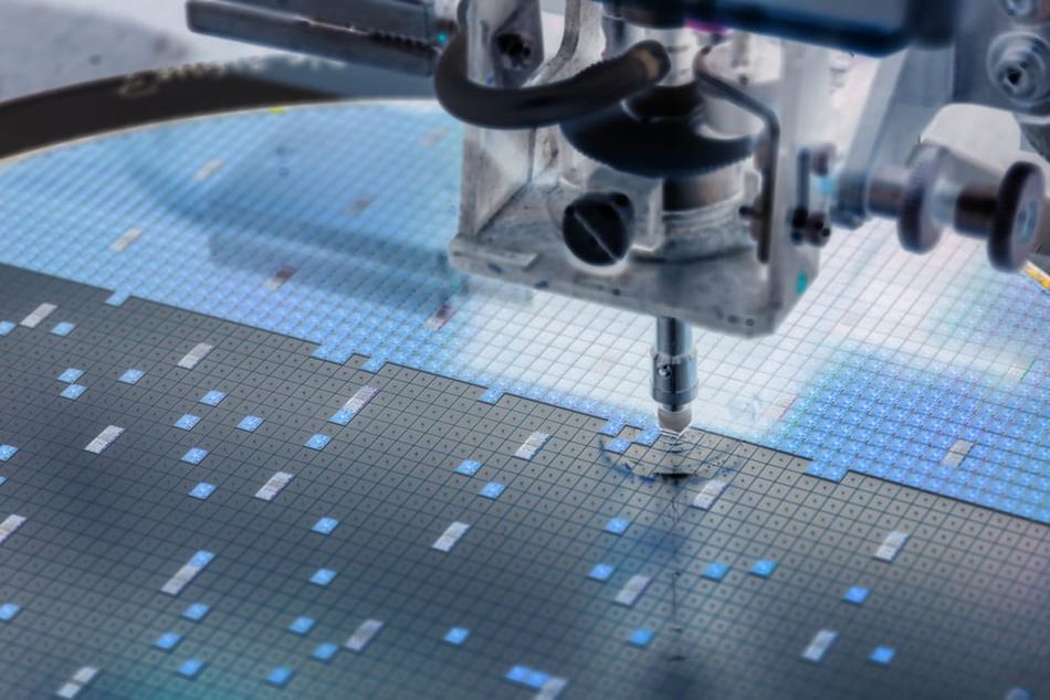
Methods for wafer thinning include mechanical grinding, chemical-mechanical planarization (CMP), wet etching, and atmospheric downstream plasma (ADP) with dry chemical etching (DCE). However, the two most common methods of wafer thinning are conventional grind and chemical-mechanical planarization.[3]
Wafer Thinning with Conventional Grind
Conventional grinding is a mechanical process of wafer thinning where a diamond and resin bonded grind wheel that is mounted on a high-speed spindle is usually employed to perform material removal. The grind recipe is what determines the spindle's speed, and is also responsible for the rate of material removal, all leading to the final intended thickness of the wafer.
Before mechanical grinding commences, a layer of grinding tape is attached to the front part of the wafer so that its contents may be insulated from damage during the thinning process. The wafer is positioned on a porous ceramic rotating vacuum chuck which serves to hold the wafer in place, with its backside facing the grind wheel. To perform the grind, the grinding wheel and the chuck rotate in opposite directions while deionized water is sprayed onto the wafer to provide cooling and wash away particles of material that came off during the grind.
This process is the most conventional thinning technique used today and is beneficial for its accuracy and high thinning rate.
Summarily, the mechanical grinding process involves 2 steps
Coarse Grinding: This is where the bulk of the material removal is done, with removal rates of around ~5μm/sec.
Fine grinding: this has a 1200 to 2000 grit sand & poligrind fine grind, which typically removes about 30µm of material accumulated from 1μm or less per second. Here is where the final finish is achieved on the wafers.[4]
Wafer Thinning with Chemical-Mechanical Planarization (CMP)
The chemical-mechanical planarization (CMP) method, also known as chemical-mechanical polishing, is performed using an abrasive chemical slurry with a polishing pad for material removal. It flattens wafers and evens out irregular topography on the surface, thus providing more planarization than the mechanical grind, but it is typically more expensive and less clean.
Chemical mechanical planarization takes place in the following steps:
-Wafer is mounted to a backside film such as a wax mount to hold it in place
-A chemical slurry is then applied and evenly distributed using a polishing pad
-The polishing pad spin is done for 60-90 seconds for each polish, depending on specifications for required thickness.
CMP's thinning rate is slower than mechanical grinding since it removes only a few microns per second. This affords the wafers near-perfect flatness and a very controlled total thickness variation (TTV).[5]
Why Do Wafers Need to be Thinned?
Ultra-compact electronic products such as microchips and handheld devices require miniature components, and the miniaturization of wafers is a pertinent step to accomplish this.
Thinned wafers are usually lighter and smaller and they make for smaller and more compact circuits that can fit into electronic devices that seem to get smaller with each new design.
Generally, electronic innovations are emerging by becoming more powerful in performance yet lighter in weight than their precursors, so For more components to fit into these devices, the semiconductors have to be smaller, tightly packed, and lighter in weight to reserve room for other elements to fit in as well. This is why wafer grinding is a critical process for the manufacturing of semiconductors.
Key Takeaways
The rapid development of miniaturized electronic devices has escalated the demand for ultra-thin silicon wafers. This is no surprising development since modern technology calls for compactness, easy mobility, and increased performance, all of which are made possible by grinding off the backside of wafers to make flexible and highly functional semiconductors.
References
1. Axus Technology. What is Wafer Grinding/Thinning? 2022. [Cited 2022 Sep 6] Available from: https://axustech.com/development-lab/grinding-thinning/#:~:text=Wafer%20backgrinding%2C%20also%20known%20as,a%20multitude%20of%20processing%20steps.
2. Pam - Xiamen. Why Wafer Thinning is Required. 2022. [Cited 2022 Sep 6] Available from: https://www.powerwaywafer.com/wafer-backside-thinning.html
3. Silicon Valley Microelectronics. Wafer Thinning. 2022. [Cited 2022 Sep 6] Available from: https://svmi.com/service/wafer-thinning/
4. Wafer World. Ultra Flat Wafers|Wafer Thinning Techniques. 2020. [Cited 2022 Sep 7] Available from: https://www.waferworld.com/post/ultra-flat-wafers-wafer-thinning-techniques
5. Silicon Valley Microelectronics. Wafer Thinning. 2022. [Cited 2022 Sep 7] Available from: https://svmi.com/service/wafer-thinning/