PCB Layers: Everything You Need to Know
PCB layers are the copper layers within a printed circuit board, laminated between or onto layers of conductive material. These layers are stacked to enhance the functionality of electronic devices. This article explores the concept of PCB layering, the various types of layers, and their benefits.

Last updated on 01 Aug, 2024. 33 minutes read
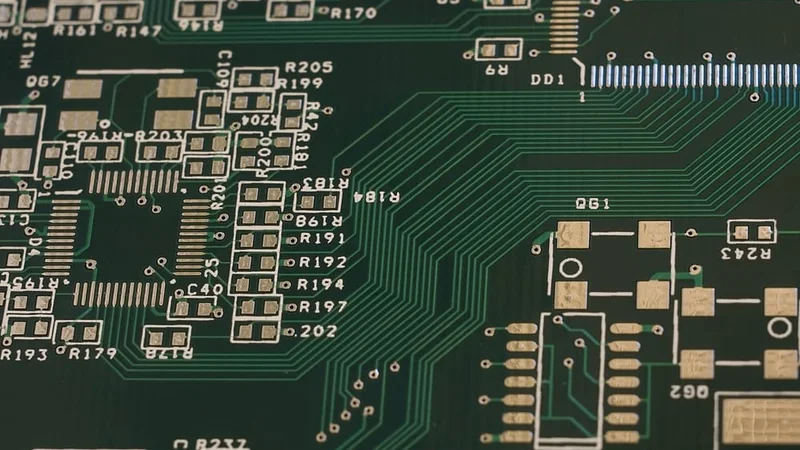
Multilayer Printed Circuit Board
Introduction
PCB layers are the different conductive and insulating sheets that make up a circuit board, each serving a specific purpose in the overall design. These layers typically include copper for conducting electricity, insulating substrates, solder masks for protection, and silkscreen for labeling.
The evolution of PCB technology has seen a dramatic shift from single-layer designs to complex multi-layer configurations. This progression has enabled the creation of increasingly powerful electronic devices while simultaneously reducing their size. The number of layers and dimensions of a particular board determines the PCB's power and capacity. As layers are added, there is increased functionality, offering vast benefits for PCB fabrication and electronics manufacturing. The ability to stack multiple layers has revolutionized circuit design, allowing for higher component density, improved signal integrity, and enhanced electromagnetic interference (EMI) shielding.
The impact of PCB layers on device miniaturization and performance cannot be overstated. By utilizing advanced layer structures, engineers can create more compact and powerful electronic products across various industries.
The Anatomy of PCB Layers: Unveiling the Hidden Complexity
PCBs are more than just their green exterior. Understanding the intricate layers beneath the surface is crucial—from copper traces that carry electrical signals to insulating dielectrics and ground planes. This knowledge helps manufacturers appreciate how these components work in concert to form the backbone of modern electronics.
Core Substrate: The Foundation of PCB Design
The core substrate serves as the foundational layer in PCB design, providing mechanical support and electrical insulation for the entire board. This critical component is typically composed of a non-conductive material that forms the base upon which conductive layers and other elements are built.
Common materials used for core substrates include FR-4 (Flame Retardant 4), a glass-reinforced epoxy laminate, and polyimide. FR-4 is widely used due to its excellent balance of electrical, mechanical, and thermal properties, as well as its cost-effectiveness. Polyimide, on the other hand, is chosen for high-temperature applications and flexible PCBs due to its superior thermal stability and flexibility.
The choice of substrate material significantly impacts PCB performance, affecting factors such as signal integrity, thermal management, and overall reliability. Engineers must carefully consider the specific requirements of their design when selecting a substrate material.
Key properties of core substrates include:
Dielectric Constant (Dk): Determines signal propagation speed and impedance. Lower Dk is preferred for high-frequency designs.
Dissipation Factor (Df): Indicates energy loss as heat. Lower Df is desirable to minimize signal attenuation.
Glass Transition Temperature (Tg): Defines the temperature at which the material transitions from a glassy to a rubbery state. Higher Tg is crucial for withstanding thermal stresses.
Coefficient of Thermal Expansion (CTE): Determines how much the material expands or contracts with temperature changes, affecting component stress and warpage.
Moisture Absorption: Impacts electrical properties and long-term reliability. Lower absorption is preferred.
Flame Retardancy: Ensures safety compliance and prevents fire spread.
Mechanical strength: Provides structural integrity to the PCB.
Copper Layers: Conducting Pathways of Electronic Signals
Copper layers are the conductive pathways in PCBs that facilitate the flow of electrical signals between components. These layers consist of thin sheets of copper foil laminated onto the core substrate, forming the basis for circuit connections. The primary functions of copper layers include signal transmission, power distribution, and heat dissipation.
The creation of copper traces and pads involves a subtractive process called etching. First, the entire copper layer is coated with a photoresist material. A negative image of the desired circuit pattern is then exposed onto the photoresist using UV light. The unexposed areas are washed away, leaving a protective layer over the intended copper traces. The board is then subjected to an etching chemical that removes the exposed copper, resulting in the final circuit pattern.
Copper thickness, often measured in ounces per square foot, significantly impacts PCB performance. Thicker copper layers offer lower resistance, improved current-carrying capacity, and enhanced heat dissipation. However, they also present challenges in achieving fine pitch traces and increase overall board weight and cost.
Copper Weight | Thickness (μm) | Current Capacity | Typical Applications |
1/2 oz | 17.5 | Low | High-density, fine-pitch designs |
1 oz | 35 | Medium | General-purpose PCBs |
2 oz | 70 | High | Power supplies, high-current applications |
3 oz | 105 | Very High | Automotive, industrial power distribution |
Recommended reading: PCB Trace: The Backbone of Modern Circuit Design
Prepreg and Laminate: Bonding the PCB Together
Prepreg (pre-impregnated) and laminate materials are essential in PCB construction, providing structural integrity and electrical insulation. Prepreg is a woven fiberglass cloth impregnated with partially cured epoxy resin, while laminate is a fully cured composite of multiple prepreg layers. In multi-layer PCBs, prepreg bonds copper foils and core materials together during lamination, where heat and pressure cause the prepreg to flow and cure, creating a unified structure. The choice of materials affects PCB characteristics like signal integrity and thermal performance, with high-speed designs often needing low dielectric constants and loss tangents to reduce signal distortion.
The lamination process for multi-layer PCBs typically involves the following steps:
Stack-up preparation: Arrange copper foils, core materials, and prepreg layers according to the PCB design.
Alignment: Ensure precise alignment of all layers using registration pins or optical systems.
Press preparation: Place the stack-up between separator plates and cushion materials.
Vacuum application: Remove air from between layers to prevent voids and ensure uniform bonding.
Heat and pressure application: Subject the stack-up to controlled temperature and pressure cycles.
Cooling: Gradually cool the laminated PCB to room temperature under controlled conditions.
Edge trimming: Remove excess material from the edges of the laminated panel.
Inspection: Perform visual and X-ray inspections to verify layer alignment and detect any defects.
Recommended reading: What is a Multilayer PCB?
Solder Mask: Protecting and Insulating PCB Surfaces
Solder mask is a critical polymer layer applied to the copper traces of a printed circuit board (PCB) to safeguard the board's integrity and functionality. Typically applied as a liquid or film, the solder mask is then cured to create a robust, protective coating.
Key functions of solder mask include:
The solder mask protects copper traces from oxidation, which can degrade electrical performance and reliability. By covering areas between closely spaced components, it reduces the risk of unintended solder bridges during assembly, preventing short circuits. It provides essential electrical insulation between conductive traces, ensuring reliable operation by preventing inadvertent short circuits. Additionally, the solder mask enhances the PCB's resistance to environmental factors such as moisture and contaminants, contributing to the board's longevity and durability. Lastly, it improves the visual appeal of the PCB by providing a uniform color and finish.
Several types of solder mask materials are available, each with unique properties:
Liquid Photoimageable (LPI): The most common type, offering excellent resolution and durability.
Dry Film: Provides uniform thickness and is suitable for fine-pitch applications.
Epoxy-based: Offers high chemical and thermal resistance.
Polyurethane: Known for its flexibility and abrasion resistance.
Lead-free compatible: Designed to withstand higher reflow temperatures.
Tips for choosing the right solder mask
When choosing the right solder mask, consider the operating environment to ensure it has appropriate chemical and thermal resistance for harsh conditions. Evaluate color requirements, as different colors can aid in visual inspection or branding, though green is traditional. Ensure the mask can reliably separate fine-pitch components by assessing the minimum solder dam. Check compatibility with the assembly process to confirm it can withstand reflow temperatures, especially for lead-free soldering. For flex or rigid-flex PCBs, choose masks with the necessary flexibility. Evaluate regulatory requirements, such as halogen-free or flame-retardant masks, if needed. Finally, balance performance with budget constraints to assess cost-effectiveness.
Recommended reading: PCB Soldermask: Everything You Need to Know
Silkscreen: Labeling and Identification Layer
The silkscreen layer, also known as the legend or nomenclature layer, is an essential component of a printed circuit board (PCB). It provides vital information for the assembly, testing, and maintenance of the PCB. This layer typically features white or yellow text and symbols that contrast with the solder mask background.
Key information included in the silkscreen layer encompasses
Component Designators: Labels such as R1 for resistor 1 or C3 for capacitor 3.
Polarity Indicators: Essential for correctly orienting polarized components like diodes and electrolytic capacitors.
Pin 1 Indicators: Critical for identifying the first pin on integrated circuits (ICs) and connectors.
Test Points and Fiducial Marks: Used for automated testing and alignment during assembly.
Manufacturer's Logo and Board Revision Number: Important for traceability and quality control.
Regulatory Compliance Symbols: Marks such as CE and RoHS to indicate compliance with relevant standards.
Warnings or Special Instructions: Instructions or cautionary notes for safe handling and assembly.
Silkscreen application techniques have advanced with PCB manufacturing technology. Traditional screen printing methods involve pushing ink through a stencil onto the board surface. However, modern techniques include:
Direct Legend Printing: Using specialized printers to apply the silkscreen directly onto the PCB.
Photoimageable Ink: Applied similarly to solder mask and then cured with UV light for precision.
Laser Marking: Utilizing lasers to etch the silkscreen onto the solder mask, offering high accuracy.
Materials used for silkscreen typically include epoxy-based inks, known for their durability and resistance to common solvents used in PCB assembly and cleaning processes. These advancements in silkscreen technology and materials ensure clear, durable, and precise labeling on PCBs, facilitating easier assembly, testing, and maintenance.
Best practices for effective silkscreen design include
When designing PCB silkscreens, prioritize readability by using clear, sans-serif fonts and appropriate text sizes. Avoid overcrowding by leaving adequate space between text and components. Ensure contrast by choosing colors that stand out against the solder mask. Maintain consistency with standardized symbols and abbreviations. Consider manufacturing tolerances to allow for potential misalignment during printing. Optimize for both machine and human readability, balancing automated assembly requirements and manual inspection needs. Include only necessary information to avoid cluttering the board with non-essential text. Align text with components so it is easily read when viewing the component. Use vector-based designs to ensure scalability and clarity of the silkscreen elements.
Recommended reading: PCB Silkscreen: What is it?
Types of PCB Layers: From Simple to Complex Configurations
Single-Layer PCBs: The Foundation of Electronic Circuits
Single-layer PCBs, also known as single-sided PCBs, represent the most fundamental form of printed circuit boards. Their simplicity and cost-effectiveness make them a cornerstone in the electronics industry, especially for high-volume, low-complexity applications.
Structure and Design
Single-layer PCBs consist of a single layer of conductive copper traces on one side of an insulating substrate, typically FR-4 or similar materials. The opposite side remains bare, serving as a mounting surface for components. The design process for these PCBs involves meticulous placement of components and routing of traces to avoid crossovers, as all connections must be made on a single plane. When crossovers are unavoidable, jumper wires or zero-ohm resistors are employed to bridge gaps.
Advantages of Single-Layer PCBs
Low Cost of Production: The straightforward manufacturing process and minimal material requirements make single-layer PCBs economical.
Simple Manufacturing Process: With only one conductive layer, the production process is simplified, reducing manufacturing time and costs.
Easier Design and Prototyping: The single-layer structure facilitates quick and straightforward design and prototyping, ideal for simple and educational projects.
Suitable for High-Volume, Low-Complexity Products: Their cost-effectiveness and simplicity make them perfect for mass-produced consumer electronics.
Good for High-Frequency Applications: The minimal signal reflection and straightforward layout can benefit high-frequency applications.
Limitations of Single-Layer Designs
Limited Circuit Density and Complexity: The single-layer design restricts the number of components and traces, limiting circuit complexity.
Challenges in Routing Complex Circuits: Complex circuits may require intricate routing, often leading to the need for larger board sizes.
Potential for Increased Board Size: Accommodating all necessary traces on a single layer can result in a larger board footprint.
Limited Suitability for High-Speed or High-Power Applications: The single-layer design lacks the necessary features to support high-speed or high-power components effectively.
Reduced Electromagnetic Interference (EMI) Shielding Capabilities: The lack of additional layers can result in insufficient EMI shielding, potentially affecting performance in sensitive applications.
Applications
Single-layer PCBs are widely used in various products, including:
Simple Consumer Electronics: Devices such as remote controls and LED lighting benefit from the low cost and simplicity of single-layer PCBs.
Household Appliances: Common household appliances like coffee makers and microwave ovens utilize single-layer PCBs for their control circuits.
Power Supplies and Adapters: Basic power supply units and adapters often feature single-layer PCBs due to their straightforward requirements.
Basic Automotive Electronics: Components like dashboard controls in vehicles rely on single-layer PCBs for their functionality.
Simple Industrial Control Systems: Industrial applications with low complexity and high-volume production use single-layer PCBs.
Educational and Hobby Electronics Kits: Single-layer PCBs are ideal for educational purposes and hobby projects, offering an easy-to-understand introduction to electronics.
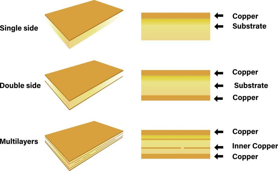
Double-Layer PCBs: Balancing Complexity and Cost
Double-layer PCBs, also known as double-sided PCBs, feature copper layers on both sides of the substrate material. This configuration allows for increased circuit density and complexity compared to single-layer designs. The two conductive layers, typically designated as the top and bottom layers, can have components mounted on one or both sides, offering greater design flexibility and performance.
Advantages of Double-Layer PCBs
Increased Circuit Density and Reduced Board Size: The use of two copper layers allows for more components and traces, reducing the overall board size.
Improved Signal Integrity: Shorter trace lengths enhance signal integrity, making double-layer PCBs suitable for high-speed applications.
Enhanced Flexibility in Component Placement and Routing: Components can be placed on both sides of the board, optimizing space and routing paths.
Better Power Distribution Capabilities: The additional layer helps in distributing power more efficiently across the board.
Improved Electromagnetic Interference (EMI) Shielding: The extra layer provides better EMI shielding, reducing noise and interference.
Role of Through-Hole Vias
Through-hole vias are a crucial element in double-layer PCB design. These are plated holes that electrically connect the top and bottom copper layers, serving multiple purposes:
Creating Electrical Connections Between Layers: Vias enable signal and power pathways between the two layers.
Allowing Components to be Mounted Through the Board: Components can be securely mounted and connected through vias.
Facilitating Heat Dissipation: Vias help in dissipating heat away from critical components.
Providing Test Points for Quality Control: Vias serve as access points for testing and quality assurance processes.
Common Applications for Double-Layer PCBs
Double-layer PCBs are widely used in various applications due to their enhanced capabilities:
Computer Motherboards and Peripherals: Increased circuit density and reliability are essential for complex computing devices.
Automotive Electronics: Engine control units and other automotive systems benefit from the robust design of double-layer PCBs.
Industrial Control Systems: These PCBs support the demands of industrial automation and control applications.
Consumer Electronics: Smartphones, tablets, and other consumer gadgets require the compact and efficient design of double-layer PCBs.
Medical Devices: Precision and reliability are critical in medical electronics, making double-layer PCBs a preferred choice.
Power Supplies and Voltage Regulators: Improved power distribution capabilities make these PCBs ideal for power-related applications.
Key Design Considerations for Double-Layer PCBs
When designing PCBs, ensure signal integrity by planning signal paths to minimize crosstalk and interference, guaranteeing clear and reliable communication. Utilize power and ground planes effectively to maintain stable voltage levels and reduce noise. Optimize component placement for efficient routing and thermal management, balancing performance and manufacturability. Strategically place vias to minimize signal degradation and maximize routing efficiency. Consider controlled impedance requirements for high-speed signals to ensure signal integrity. Design an appropriate layer stackup for the intended application, balancing performance and manufacturability. Account for heat dissipation in component placement and copper distribution to avoid overheating. Adhere to design rules for minimum trace widths, spacings, and via sizes to ensure manufacturability. Balance design complexity with manufacturing costs to achieve cost-effective solutions. Implement proper grounding and shielding techniques to minimize electromagnetic interference.
Multi-Layer PCBs: Powering Advanced Electronics
Multi-layer PCBs consist of three or more conductive layers separated by insulating material, allowing for intricate circuit designs in a compact form factor. Common configurations include 4-layer, 6-layer, 8-layer, and even higher layer counts for extremely dense designs. This advanced structure offers several significant benefits that make multi-layer PCBs essential in modern electronics.
2 Layer PCB
A 2-layer PCB, or double-sided PCB, features copper coatings on both sides with an insulating layer in between. Components can be mounted on both sides. These PCBs are fabricated by joining two copper layers with a dielectric material in between. The copper layers transmit different electrical signals, making them suitable for high-speed, compact applications. The dielectric material prevents signal interference. They are common and economical to manufacture. An example is simple LED circuit board.
4 Layer PCB
A 4-layer PCB has four conductive layers: top, two inner (usually for power and ground), and bottom layers. The top and bottom layers are used for components and signal routing, while the inner layers provide stable power and ground planes. Vias connect these layers, ensuring signal integrity and improved thermal management. This stack-up can be adjusted based on design needs, making 4-layer PCBs versatile and advantageous over 2-layer PCBs. An example is a power supply board.
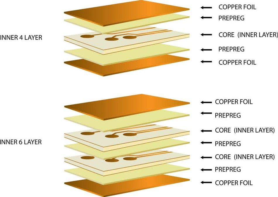
6 Layer PCB
A 6-layer PCB extends a 4-layer board by adding two extra signal layers between the planes. This stack-up includes four routing layers and two internal planes for ground and power. The design helps manage EMI by separating high-speed and low-speed signal layers. The standard stack-up includes top layer, prepreg, internal ground plane, core, internal routing layers, internal power plane, and bottom layer. Adjustments can be made for routing efficiency and minimizing crosstalk. An example is a medical device.
8 Layer PCB
An 8-layer PCB features four signal layers and four planes (ground and power). This configuration minimizes crosstalk and enhances signal traces, making it suitable for complex, compact devices. The stack-up improves routing quality, power and ground plane separation, and EMC performance. These PCBs also handle high current traces with low impedance, making them efficient for high-speed signal routing. An example is advanced graphics card.
Advantages of Multi-Layer PCBs
Increased Circuit Density and Functionality: The multiple layers allow for more complex circuits and a higher number of components, increasing the overall functionality of the PCB.
Improved Signal Integrity and Reduced Electromagnetic Interference (EMI): The additional layers help to minimize signal degradation and reduce EMI, essential for high-speed and high-frequency applications.
Enhanced Power Distribution and Thermal Management: Dedicated power and ground planes provide efficient power distribution and effective thermal management, ensuring stable operation of the circuit.
Reduced Board Size and Weight: The compact design of multi-layer PCBs enables smaller and lighter devices, a crucial factor in modern electronics.
Greater Design Flexibility for Complex Systems: The layered structure allows for more sophisticated routing and placement of components, accommodating complex system requirements.
Functions of Inner Layers
In multi-layer PCBs, inner layers serve crucial functions beyond signal routing. Power planes and ground planes are dedicated layers that provide low-impedance power distribution and return paths, respectively. These planes offer several advantages:
Reduced Power Supply Noise and Improved Signal Integrity: Power and ground planes help stabilize voltage levels and minimize noise, improving overall signal quality.
Lower Inductance for High-Speed Signals: The close proximity of power and ground planes reduces inductance, which is beneficial for high-speed signal transmission.
Enhanced EMI Shielding: Inner layers act as shields against electromagnetic interference, protecting sensitive signals.
Improved Thermal Dissipation: The copper planes facilitate better heat dissipation, preventing overheating of critical components.
Simplified Routing of Signal Layers: Dedicated power and ground layers free up other layers for signal routing, simplifying the design process.
Advanced Via Technologies
Multi-layer PCBs utilize advanced via technologies to interconnect layers, each serving specific purposes:
Through-Hole Vias: These vias extend through all layers of the board, providing robust connections across the entire PCB.
Blind Vias: Blind vias connect an outer layer to one or more inner layers without passing through the entire board, saving space and reducing potential signal loss.
Buried Vias: Buried vias connect inner layers without extending to the outer layers, optimizing the use of board space and improving signal integrity.
Recommended reading: PCB Via: What is a Via?
Layer Count | Typical Applications | Key Features |
2-layer | Simple consumer electronics, basic LED circuits | Cost-effective, minimal complexity |
4-layer | Consumer electronics, automotive systems | Balance of complexity and cost |
6-layer | Industrial controls, medical devices | Improved signal integrity, dedicated power/ground planes |
8-layer | Telecommunications, high-speed computing | Enhanced EMI control, complex routing capabilities |
10+ layer | Aerospace, advanced military systems | Extreme density, superior signal integrity, advanced thermal management |
High-Density Interconnect (HDI) PCBs: Pushing the Boundaries of Miniaturization
High-Density Interconnect (HDI) PCBs represent the cutting edge of printed circuit board technology, designed to meet the demands of increasingly compact and complex electronic devices. Characterized by their higher circuitry density per unit area, HDI PCBs achieve this through advanced manufacturing techniques and design principles, making them essential for modern electronics.
Key Features of HDI PCBs
Microvias: Featuring diameters less than 150 μm, microvias enable high-density interconnections.
Ultra-Fine Line Width and Spacing: Typically less than 100 μm, these fine lines allow for more intricate circuit patterns.
Higher Connection Pad Density: Increased pad density supports more components in a given area.
Increased Layer Count: More layers in a thinner overall profile facilitate complex circuit designs.
Advanced Materials: Enhanced electrical and thermal performance through the use of sophisticated materials.
Advanced Manufacturing Techniques
The production of HDI PCBs involves several cutting-edge manufacturing techniques:
Laser Drilling: Precise creation of microvias and blind vias, crucial for high-density designs.
Sequential Lamination: Building up the PCB structure layer by layer to achieve the desired complexity.
Photoimageable Dielectrics: Enabling finer line resolution and smaller vias, critical for high-density circuitry.
Advanced Plating Techniques: Ensuring reliable connections in high-aspect-ratio vias.
Optical Alignment Systems: Maintaining precise registration between layers for accurate circuit construction.
Benefits of HDI PCBs
HDI PCBs offer significant advantages in terms of signal integrity and component density:
1. Improved Signal Integrity:
Improved signal integrity in HDI PCBs is achieved through shorter signal paths that reduce propagation delays and reflections, smaller vias that minimize stub effects and impedance discontinuities, and dedicated power and ground planes that reduce noise and crosstalk, enhancing signal clarity.
2. Enhanced Component Density:
Enhanced component density in HDI PCBs is achieved through efficient use of board space with microvias for better component placement, finer line widths and spacings for more traces between components, and increased layer count for accommodating complex routing in a smaller area, supporting advanced designs.
Applications
Modern electronics applications span a wide range of industries, driving innovation and performance. Smartphones and tablets integrate multiple functions in slim form factors, while wearable devices focus on miniaturization for comfort and aesthetics. Advanced medical implants require compact, high-reliability designs for critical applications. 5G communication equipment meets the demands of high-frequency, high-bandwidth systems. Automotive ADAS integrates complex sensor and processing capabilities, and AI and ML hardware supports dense, high-performance computing modules. In aerospace and defense, sophisticated, lightweight electronic warfare and communication systems are made possible.
Design Considerations for PCB Layers: Optimizing Performance and Manufacturability
Stack-Up Design: Balancing Signal Integrity and EMI Control
PCB stack-up design is a pivotal element in the development of multi-layer printed circuit boards (PCBs), profoundly influencing the board's electrical performance, manufacturability, and overall cost. It involves the strategic arrangement of conductive and dielectric layers to optimize signal integrity, control impedance, and mitigate electromagnetic interference (EMI). A meticulously designed stack-up forms the foundation for a high-performance PCB, ensuring that the board meets its electrical and mechanical requirements while remaining cost-effective to manufacture.
Importance of Stack-Up Design
The significance of stack-up design cannot be overstated as it directly impacts:
Signal Propagation: Affects how signals travel across the board, influencing speed and reliability.
Crosstalk: Minimizes interference between adjacent traces, crucial for maintaining signal clarity.
Power Distribution Efficiency: Ensures stable power supply across the board.
EMI Profile: Reduces electromagnetic emissions and susceptibility to external interference.
Key Factors in Stack-Up Design
Impedance Control: Maintaining consistent impedance is essential for preserving signal integrity, especially in high-speed designs. This requires careful management of trace widths, dielectric thicknesses, and material properties.
EMI Shielding: Proper placement can significantly reduce electromagnetic emissions and improve immunity to external interference.
Signal Layer Pairing: Arranging signal layers next to reference planes helps maintain signal integrity and reduce crosstalk.
Dielectric Material Selection: Choosing suitable dielectric materials is crucial for achieving the desired electrical and mechanical properties.
Manufacturability: Considering aspect ratios, copper weights, and board thickness ensures the design can be reliably manufactured.
Guidelines for Effective Stack-Up Design in Multi-Layer PCBs
These include maintaining a symmetrical design to minimize warpage, placing high-speed signals on inner layers adjacent to uninterrupted reference planes to maintain signal integrity. Others include alternating signal and plane layers to reduce loop inductance and improve signal quality, achieving better impedance control by tightly coupling signal layers with their adjacent planes, enhancing power integrity with buried capacitance layers, maintaining consistent dielectric thicknesses for uniform electrical performance, utilizing different dielectric materials for specific electrical characteristics, and ensuring adequate isolation between noisy digital circuits and sensitive analog sections to prevent interference.
Impedance Control: Ensuring Signal Quality Across Layers
Impedance control has evolved alongside the increasing speeds of electronic systems, becoming a fundamental aspect of modern PCB design. Since the emergence of high-speed digital circuits in the 1970s, engineers have faced the challenge of maintaining signal integrity as frequencies and edge rates have escalated. Today, impedance control is essential for the reliable operation of a wide array of electronic systems, from smartphones to satellite communications.
Core Concept
At its essence, impedance control involves managing the characteristic impedance of transmission lines within a PCB to maintain signal integrity and minimize reflections. As signal frequencies rise and edge rates become faster, this management becomes increasingly critical. Controlled impedance is vital for preserving signal quality, reducing electromagnetic interference (EMI), and ensuring the functionality of high-speed digital and RF circuits.
Influence of PCB Layer Configuration
The configuration of PCB layers is pivotal in determining and controlling impedance. Several factors influence the characteristic impedance of a trace:
Trace Width and Thickness: Directly affects impedance.
Dielectric Material Properties: The material's dielectric constant influences impedance.
Distance to Reference Planes: Affects impedance based on trace proximity to reference planes.
In multi-layer PCBs, the stack-up design significantly impacts these parameters, affecting the impedance of traces on various layers. For instance:
Dielectric Thickness: A thicker dielectric generally results in higher impedance, while traces closer to their reference planes have lower impedance and improved coupling.
Dielectric Material: Materials with lower dielectric constants typically yield higher impedance for a given trace geometry.
Engineers achieve controlled impedance in PCB designs through various techniques. These include precise stack-up planning to ensure consistent dielectric thickness and material properties, trace width control based on layer and surrounding conditions, the use of coplanar waveguide structures for improved impedance control in microwave designs, and differential pairs routing to maintain consistent spacing and symmetry. Poor impedance control can lead to signal reflections, causing data errors and increased EMI, timing errors, reduced noise margins, and increased bit error rates in high-speed digital systems, and power loss, reduced sensitivity, and degraded performance in RF and microwave circuits.
To illustrate the precision required in impedance control, consider the formulas used for calculating trace impedance in different PCB configurations:
For a microstrip (surface layer trace): Z₀ = [87 / (√(εr + 1.41))] * ln(5.98h / (0.8w + t))
And for a stripline (inner layer trace): Z₀ = [60 / √εr] * ln[1.9b / (0.8w + t)]
Where:
Z₀ is the characteristic impedance.
εr is the dielectric constant of the substrate.
h is the height of the trace above the ground plane.
w is the width of the trace.
t is the thickness of the trace.
b is the distance between two ground planes in a stripline configuration.
These formulas provide a starting point but often fall short in capturing the complexity of modern PCB designs. As a result, electromagnetic field solvers and advanced simulation tools have become indispensable for precise impedance control, especially in intricate multi-layer designs where layer interactions significantly impact impedance characteristics.
Recommended reading: Controlled Impedance: A Comprehensive Guide
Power Distribution: Optimizing Power and Ground Planes
Effective power distribution is crucial for the reliable operation of multi-layer PCBs, especially as digital circuits become faster and more complex. Proper power distribution minimizes voltage drops, reduces electromagnetic interference (EMI), and maintains signal integrity across the board. The cornerstone of this process is the strategic design of power and ground planes, which play a vital role in ensuring clean and stable power delivery.
Role of Power and Ground Planes
Power and ground planes are dedicated layers in a PCB that provide low-impedance paths for current flow and stable voltage references for all components. Well-designed power and ground planes can significantly enhance system performance by:
Reducing Power Supply Noise: By providing stable voltage and minimizing fluctuations.
Minimizing Ground Bounce: Through effective grounding practices.
Enhancing EMI Shielding: By creating barriers against electromagnetic interference.
Strategies for Optimizing Power Distribution
Layer Stack-Up Optimization: Place power and ground planes close to each other to create a low-inductance power delivery network. This arrangement functions as a built-in capacitor, helping to suppress high-frequency noise.
Plane Segmentation: Divide power planes into distinct regions for different voltage levels or sensitive analog sections. This technique isolates noise-sensitive circuits from potential interference sources.
Copper Pour Utilization: Use copper pours on signal layers connected to power or ground to enhance the effective plane area and reduce impedance.
Via Stitching: Implement frequent vias to connect power and ground planes, which reduces plane impedance and improves current return paths.
Minimizing Power Supply Noise and Ground Bounce
To minimize power supply noise and ground bounce, strategically place decoupling capacitors near IC power pins to provide local charge storage and reduce high-frequency noise. Use LC filters at power entry points to filter incoming noise and ensure clean power for sensitive circuits. Employ continuous ground planes to minimize impedance and ground bounce. Size power planes adequately to handle the required current without significant voltage drop. Design power distribution networks with controlled impedance to match source and load impedances, thereby reducing reflections and noise.
Best Practices for Power Distribution Design
Best practices for power distribution design include hierarchical distribution of capacitors, with bulk capacitors at power entry points and smaller decoupling capacitors near ICs. Use wide, short traces for power connections to minimize resistance and inductance. Avoid routing high-speed signals across splits in power or ground planes to prevent interference. Employ guard traces to isolate sensitive analog signals from digital noise. Consider embedded capacitance layers for high-frequency decoupling and perform post-layout simulations to verify power integrity. Use thermal relief connections for power pins to balance thermal management and manufacturability. Implement separate analog and digital ground planes connected at a single point to avoid ground loops. Use power islands for voltage regulators or high-current devices to manage thermal dissipation, and utilize power integrity analysis tools to optimize capacitor placement and values.
Signal Routing: Navigating the Maze of PCB Layers
In multi-layer PCB design, efficient signal routing is akin to navigating a complex maze, requiring a deep understanding of electromagnetic principles, manufacturing constraints, and design trade-offs. A well-planned layer stack-up is crucial, often dedicating layers to different signal types—high-speed signals on layers adjacent to ground planes, power distribution on inner layers for EMI reduction, and critical signals on internal layers for protection against interference. Strategies such as "microvia" technology and "blind" or "buried" vias enhance routing flexibility and reduce signal path lengths. Signal integrity, which involves maintaining waveform quality and reliable information transmission, is critical. This requires precise control of trace widths and spacings to achieve consistent impedance and manage return paths effectively. Continuous reference planes and careful management of return currents prevent signal reflections and EMI. Techniques to minimize crosstalk and EMI include increasing trace spacing, using orthogonal routing, implementing guard traces, and employing differential pair routing for high-speed signals to improve noise immunity.
EMI reduction strategies
EMI reduction strategies include minimizing loop areas in signal paths to reduce the antenna effect, using ground planes to shield signals and provide low-impedance return paths, and implementing EMI suppression components such as ferrite beads at board edges or near connectors. Managing high-speed signals in multi-layer PCBs presents unique challenges, as higher frequencies make traces behave like transmission lines, requiring careful consideration of signal propagation. Key tips include maintaining consistent impedance along the entire signal path, using shorter trace lengths to minimize signal degradation and EMI susceptibility, and implementing proper termination techniques to prevent signal reflections. Specialized PCB materials with lower dielectric loss can benefit critical high-speed sections, while advanced routing techniques like serpentine routing for length matching in differential pairs and simulation tools for analyzing signal integrity are also essential for making informed design decisions.
Manufacturing Processes for PCB Layers: From Design to Reality
Photolithography: Precision Patterning of PCB Layers
Photolithography, a key process in modern PCB manufacturing, has evolved from its photographic origins to enable the precise creation of complex circuit boards. This technique involves transferring a pattern from a photomask onto a photosensitive photoresist layer on the PCB surface.
Process Overview
Photoresist Application: A light-sensitive layer (positive or negative) is coated onto the PCB’s copper surface.
Mask Alignment: A photomask with the desired circuit pattern is aligned over the board.
UV Exposure: Intense UV light exposes the photoresist through the mask, altering it chemically.
Development: The soluble photoresist is washed away, revealing the underlying copper pattern.
Etching: Exposed copper is etched away, leaving the final circuit design.
Resist Stripping: Remaining photoresist is removed.
Inspection: The pattern is checked for accuracy.
Importance of Mask Alignment
In multi-layer PCBs, precise mask alignment is crucial to ensure correct positioning of vias and interconnects. Misalignment can cause connection issues or short circuits. Modern facilities use advanced optical systems and fiducial markers to achieve high precision.
Key Stages
Surface Preparation: Clean and level the board.
Pre-bake: Dry the photoresist for better adhesion.
UV Exposure: Transfer the mask pattern to the photoresist.
Development and Etching: Reveal and etch the copper pattern.
Resist Stripping and Inspection: Finalize and verify the board.
Drilling and Plating: Creating Interconnections Between Layers
The evolution of multi-layer PCBs is closely tied to advancements in drilling and plating technologies. These critical processes have seen significant refinements since the 1950s, enabling the production of complex boards with densely packed components. Drilling, which involves creating precise holes through the board layers, has advanced from manual methods to computer-controlled systems capable of producing thousands of holes per minute with micron-level accuracy. High-speed CNC machines with specialized drill bits are now used to minimize burring and ensure clean, precise holes.
The types of holes created in PCBs serve different purposes and present unique manufacturing challenges:
Through-holes: They are the most straightforward to manufacture but occupy space on all layers.
Blind vias: They allow for higher component density by freeing up space on internal layers.
Buried vias: They offer the highest density routing options but are the most complex to manufacture.
The advent of laser drilling has revolutionized the creation of micro-vias, enabling hole diameters as small as 50 microns. This technology has been crucial in supporting the trend towards miniaturization in electronics.
Once holes are drilled, the plating process creates electrical connections between layers. This process has its roots in electroplating techniques developed in the 19th century but has been refined for PCB manufacturing. The basic steps involve cleaning the holes, catalyzing the surfaces to promote copper adhesion, and then electroplating copper onto the hole walls.
The plating process begins with a thin layer of electroless copper deposition, which provides a conductive base layer for subsequent electroplating. This is followed by electrolytic copper plating, which builds up the copper thickness to the required specifications. Advanced techniques like pulse plating and reverse pulse plating have been developed to improve the uniformity and reliability of the copper layer, especially in high aspect ratio holes.
Table: Comparison of Drilling and Plating Techniques
Technique | Advantages | Limitations | Typical Applications |
Mechanical Drilling | Cost-effective for larger holes, high throughput | Limited minimum hole size (typically >0.2mm), tool wear | Through-holes, larger vias |
Laser Drilling | Very small hole sizes possible (<100μm), no tool wear | Higher cost, limited to certain materials | Micro-vias, high-density interconnects |
Electroless Plating | Uniform deposition, good for high aspect ratio holes | Slower deposition rate, more expensive | Initial conductive layer for all hole types |
Electrolytic Plating | Fast deposition, cost-effective for bulk copper | Requires conductive seed layer, can be non-uniform in high aspect ratio holes | Main copper build-up for all hole types |
Direct Metallization | Eliminates need for electroless copper, environmentally friendly | Limited to certain board materials, may have adhesion issues | Alternative to traditional electroless/electrolytic process |
Lamination: Bonding PCB Layers into a Unified Structure
Lamination is a pivotal stage in multi-layer PCB manufacturing where individual layers are fused into a cohesive unit. Since its inception in the 1960s, the process has evolved with advancements in materials and technology.
Lamination Process
Lamination involves stacking copper-clad cores and prepreg (epoxy-impregnated glass cloth) layers. This stack is heated and pressed in a vacuum environment to bond the layers, preventing air entrapment that could cause delamination.
Key Factors
Alignment: Accurate layer alignment is crucial to avoid disconnected vias and compromised signal integrity. Modern systems use optical alignment and precision pins to ensure correct positioning.
Pressure Control: Proper pressure is essential. Too little pressure can cause incomplete bonding and voids, while too much can distort traces and prepreg flow. Advanced systems use computer-controlled presses to dynamically adjust pressure based on board thickness and design.
Prepreg plays a pivotal role in the lamination process. These sheets of glass cloth impregnated with partially cured epoxy resin serve multiple functions:
Bonding agent: When heated, the resin in the prepreg flows and then cures, effectively gluing the layers together.
Dielectric material: Prepreg provides electrical insulation between conductive layers.
Planarization: It helps to fill in and smooth out surface irregularities on copper layers.
Thickness control: The number and thickness of prepreg layers can be adjusted to achieve the desired overall board thickness.
The characteristics of the prepreg, including resin content, flow behavior, and glass transition temperature, significantly influence the lamination process and final board properties. To ensure successful lamination in complex multi-layer designs, optimize material selection by choosing prepreg and core materials with compatible thermal and mechanical properties. Implement a proper stack-up design by alternating the orientation of adjacent prepreg layers to minimize warpage, and use sacrificial copper layers that can be etched away post-lamination to improve planarity. Control moisture content by properly drying materials before lamination to prevent outgassing and delamination. Employ simulation tools, such as thermal and pressure software, to optimize lamination parameters, and consider step lamination for very thick boards to ensure uniform bonding. Utilize vacuum assistance to maintain a proper vacuum and minimize void formation, optimize cooling rates to reduce internal stresses, and implement post-lamination stress relief with a separate thermal cycle to address internal stresses after initial lamination.
Surface Finishing: Protecting and Preparing PCB Layers
Surface finishing is a crucial final step in PCB manufacturing that protects exposed copper and prepares the board for component assembly. Since the early days of PCB production, this process has evolved to meet the increasing demands for reliability, performance, and environmental compliance.
Types of Surface Finishes
Hot Air Solder Leveling (HASL): Previously the industry standard, HASL provides good solderability and affordability but has limitations in flatness and lead content.
Electroless Nickel Immersion Gold (ENIG): Known for excellent flatness and compatibility with fine-pitch components, ENIG is preferred for its reliability but is more expensive and can suffer from "black pad" syndrome.
Immersion Silver and Immersion Tin: These cost-effective finishes offer good solderability and lead-free compatibility. They are prone to tarnishing and oxidation and require careful handling.
Organic Solderability Preservatives (OSP): This thin organic coating preserves copper solderability, making it ideal for high-volume, cost-sensitive applications, though it has limitations with multiple reflow cycles and shelf life.
Impact on PCB Performance
Solderability: Ensures proper component attachment and electrical connections. ENIG and Immersion Silver provide excellent initial solderability, while HASL is robust but challenging for fine-pitch components.
Long-term Reliability: Affects oxidation resistance, intermetallic compound formation, and thermal cycling performance. ENIG, for example, excels in oxidation resistance and long-term solderability.
Recommended reading: PCB Surface Finish: The Ultimate Guide to Understanding and Choosing the Right Option
Table: Comparison of PCB Surface Finish Options
Finish Type | Pros | Cons | Solderability | Shelf Life | Flatness | Typical Applications |
HASL (Lead) | Good solderability, low cost | Poor flatness, contains lead | Excellent | Good | Poor | General-purpose electronics |
Lead-Free HASL | Lead-free, good solderability | Poor flatness, higher processing temperatures | Very Good | Good | Poor | Consumer electronics |
ENIG | Excellent flatness, good for fine pitch | Higher cost, potential for 'black pad' | Good | Excellent | Excellent | High-reliability electronics, fine-pitch components |
Immersion Silver | Good solderability, fine-pitch compatible | Prone to oxidation, careful handling required | Very Good | Moderate | Very Good | Telecommunications, computer hardware |
Immersion Tin | Good solderability, low cost | Prone to whisker growth, shorter shelf life | Good | Moderate | Good | Consumer electronics, automotive |
OSP | Low cost, environmentally friendly | Limited reflow cycles, shorter shelf life | Good | Poor | Excellent | High-volume consumer products |
Testing and Quality Control of PCB Layers: Ensuring Reliability and Performance
Electrical Testing: Verifying Connectivity and Isolation
Electrical testing is critical in PCB manufacturing for verifying electrical connections and ensuring proper isolation between circuits. Modern techniques now rapidly and accurately assess complex multi-layer boards, evolving from the early days of manual point-to-point testing.
Two primary methods dominate PCB electrical testing: flying probe and bed of nails. Flying probe testing uses mobile probes to contact test points, checking for continuity and isolation. This method is flexible and ideal for prototypes or low-volume production, as it requires no custom fixtures. Bed of nails testing employs a fixed array of spring-loaded pins to contact multiple test points simultaneously, offering extremely fast test cycles suitable for high-volume production, though it requires a custom fixture for each board design.
In multi-layer PCBs, continuity and isolation testing are crucial due to the increased complexity of interconnections. Continuity testing verifies that all intended connections are properly made, ensuring the integrity of vias, plated through-holes, and copper traces across different layers. Isolation testing confirms there are no unintended connections or short circuits between adjacent traces or planes, preventing crosstalk and ensuring proper circuit function.
As PCB designs have grown more complex, with higher densities and the incorporation of HDI (High-Density Interconnect) technologies, advanced testing techniques have emerged. These include:
Boundary scan testing (JTAG): Uses built-in test circuitry to assess connections on densely populated boards.
Capacitive testing: Detects opens and shorts in fine-pitch components where physical probe access is limited.
Automated Optical Inspection (AOI): While primarily for visual defects, advanced AOI systems can detect some electrical issues.
4-wire Kelvin testing: Provides highly accurate resistance measurements for critical connections.
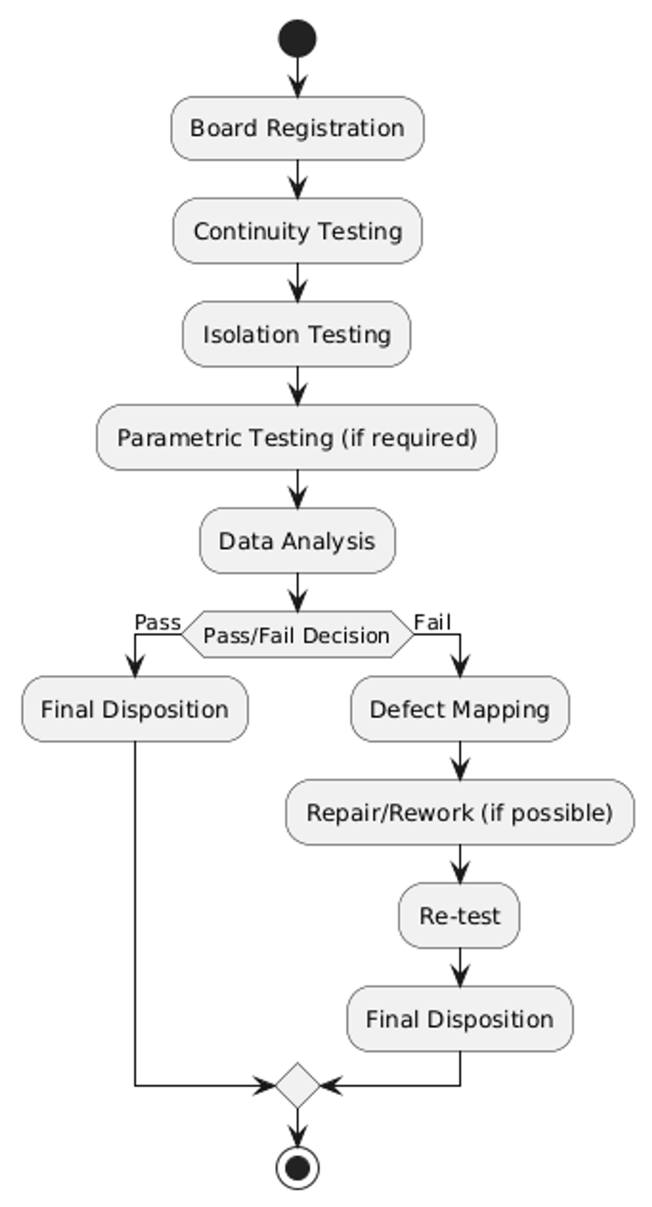
Flowchart of a typical PCB electrical testing process:
X-ray Inspection: Peering Inside Multi-Layer PCBs
X-ray inspection has become an indispensable tool in multi-layer PCB quality control, offering a non-destructive means of examining internal structures and hidden solder joints. This technology, adapted from medical and industrial applications, provides invaluable insights into the internal integrity of PCBs, particularly as designs have grown more complex and components more densely packed.
X-ray inspection in PCB manufacturing primarily focuses on detecting defects that are not visible through optical inspection methods. These include:
Voids in solder joints, particularly in BGA (Ball Grid Array) and QFN (Quad Flat No-lead) packages
Misalignment of internal layers
Broken or insufficiently filled vias and through-holes
Delamination between layers
Trace breaks or shorts in inner layers
Foreign material inclusions
The advantages of X-ray inspection are numerous. It allows for the examination of hidden solder joints, crucial for BGA and other area-array packages. It can detect internal defects before they lead to field failures, enhancing overall product reliability. X-ray systems can also perform automated inspection at high speeds, making them suitable for in-line production testing.
However, X-ray inspection does have limitations. The resolution of X-ray images can be affected by the overall board thickness and the presence of high-density materials. Interpretation of X-ray images often requires skilled operators, as some defects can be subtle or easily misinterpreted. Additionally, while X-ray inspection can detect the presence of defects, it may not always provide information about the root cause.
Recommended reading: PCB Inspection: Ensuring Quality and Reliability in Electronics Manufacturing
Thermal Stress Testing: Evaluating Layer Integrity Under Heat
Thermal stress testing is essential for multi-layer PCB qualification, reflecting the harsh realities of modern electronic environments. As devices become more compact and powerful, thermal challenges have intensified, making this testing crucial for ensuring long-term reliability and performance. It simulates real-world conditions, including operational heat, environmental temperature fluctuations, and thermal shock from manufacturing processes like soldering. Controlled thermal stress helps identify potential weaknesses in design or materials before they cause field failures. Various methods are employed to evaluate different aspects of PCB resilience.
Reflow Simulation: This method mimics the soldering process, subjecting the PCB to temperatures that can exceed 250°C. It's crucial for evaluating the board's ability to withstand assembly processes without delamination or warpage.
Thermal Cycling: PCBs are exposed to alternating extreme temperatures, often ranging from -65°C to +150°C. This test assesses the board's ability to withstand repeated expansion and contraction, which can stress solder joints and internal connections.
Thermal Shock: Similar to thermal cycling but with more rapid temperature changes, this test evaluates the PCB's resistance to sudden thermal stress, which can cause immediate failures or accelerate long-term degradation.
Power Cycling: By rapidly switching power on and off, this test simulates the thermal stress of regular device usage, particularly important for components that generate significant heat.
Regular device usage, especially for heat-generating components, can significantly impact PCB integrity and performance, leading to issues such as delamination, warpage, via failure, copper fatigue, and component stress due to thermal expansion. To design PCBs that withstand thermal stress, use materials with matched Coefficients of Thermal Expansion (CTE), implement proper via design including tenting and filling for critical connections, and utilize thermal relief pads for large components. Consider embedded components for critical circuits, balance copper across layers to minimize warpage, use stiffeners or core materials with high glass transition temperatures (Tg), optimize component placement to distribute heat sources evenly, and implement thermal management techniques like heat sinks or thermal vias.
Signal Integrity Testing: Ensuring High-Speed Performance
Signal integrity testing has become increasingly crucial as PCB designs push into higher frequencies and data rates. This form of testing ensures that signals maintain their intended characteristics as they propagate through the PCB, a challenge that grows more complex with each increase in speed and density.
The concept of signal integrity involves ensuring correct timing, maintaining voltage levels, preserving waveform shape, and minimizing noise. Common issues in multi-layer PCBs include crosstalk, reflections, attenuation, jitter, ground bounce, and electromagnetic interference (EMI). To evaluate signal integrity, techniques like Time Domain Reflectometry (TDR), Vector Network Analysis (VNA), Eye Diagram Analysis, Bit Error Rate Testing (BERT), and Near-End and Far-End Crosstalk (NEXT/FEXT) testing are used.
Improving signal integrity involves implementing controlled impedance routing, using ground planes adjacent to signal layers, minimizing via transitions, employing differential signaling, using proper termination techniques, matching trace lengths, optimizing trace geometries, and ensuring a well-designed power distribution network (PDN). Simulation tools during the design phase can help predict and mitigate potential issues.
Conclusion
The intricate world of PCB layers forms the backbone of modern electronics, enabling the creation of increasingly complex and compact devices. From single-layer boards to high-density interconnect (HDI) PCBs, layer technology has been pivotal in advancing electronic capabilities. Critical aspects of PCB layer design and manufacturing include stack-up design, impedance control, and power distribution, which are crucial for optimal performance and reliability. Advanced manufacturing processes such as precise photolithography, drilling, and plating techniques have expanded the possibilities in PCB production.
Rigorous testing and quality control—like electrical testing, X-ray inspection, thermal stress evaluation, and signal integrity analysis—are essential to ensure functionality and longevity. For engineering professionals, mastering PCB layer technology is imperative as electronics continue to advance and design challenges grow more complex. By understanding layer structures, materials, and manufacturing processes, engineers can innovate effectively, creating high-performance, reliable designs. As you embark on your next PCB design project, apply this knowledge to make informed decisions about stack-up design, material selection, and manufacturing processes. Each layer, via, and trace plays a vital role in the final product's performance, and a comprehensive understanding of PCB layer technology will help you create designs that meet current demands and pave the way for future advancements.
Frequently Asked Questions
Q: What is the maximum number of layers that can be used in a PCB?
A: There's no strict technical limit to the number of layers in a PCB. While most commercial PCBs range from 1 to 16 layers, some advanced applications use boards with 30, 50, or even 100+ layers. However, as layer count increases, so do manufacturing complexity, cost, and potential for defects.
Q: How does the choice of PCB layer count affect signal integrity?
A: Higher layer counts generally allow for better signal integrity by providing more options for shielding, controlled impedance routing, and power/ground plane placement. This can reduce crosstalk, EMI, and allow for cleaner signal transmission. However, more layers also mean more vias, which can introduce their own signal integrity challenges.
Q: Are thicker PCBs always better for heat dissipation?
A: This is a common misconception. While thicker PCBs can sometimes help with heat dissipation, the effectiveness depends more on the design and materials used. Proper use of thermal vias, copper pours, and choosing materials with good thermal conductivity are often more effective than simply increasing board thickness.
Q: How do blind and buried vias affect PCB manufacturing cost?
A: Blind and buried vias typically increase manufacturing cost due to the additional processing steps required. They necessitate sequential lamination processes and more complex drilling operations. However, they can allow for higher component density and improved signal routing, which might justify the cost in high-performance applications.
Q: Can different dielectric materials be used within the same multi-layer PCB?
A: Yes, it's possible and sometimes desirable to use different dielectric materials within the same PCB. This technique, known as hybrid stack-up, can optimize performance by using high-speed materials for critical signal layers while using standard FR-4 for less critical layers to manage costs.
Q: How does the number of layers in a PCB affect its flexibility?
A: Generally, PCBs become less flexible as the number of layers increases. This is due to the increased thickness and the cumulative rigidity of multiple layers. Flex and rigid-flex PCBs use specialized materials and designs to maintain flexibility even with multiple layers, but there are still practical limits to the number of layers that can be used in flexible applications.
Q: What's the difference between a ground plane and a power plane in multi-layer PCBs?
A: While both are continuous copper layers, a ground plane provides a return path for signals and helps with EMI shielding, typically maintained at 0V. A power plane distributes power throughout the board, maintained at a specific voltage (e.g., 3.3V, 5V). Using dedicated planes for ground and power helps reduce noise and improves signal integrity.
Reference
1. PCBA Store. Everything About Printed Circuit Board (PCB) Layers. 2020. Available from: https://www.pcbastore.com/blogs/printed-circuit-board-layers-explained.html
2. The Engineering Projects. Introduction to Single-Layer PCB. 2021. Available from: https://www.google.com/amp/s/www.theengineeringprojects.com/2021/11/introduction-to-single-layer-pcb.html/%3famp=1
3. Electronics And You. Multilayer PCB| Types of PCB| Design, Tutorial, Manufacturing Process. 2021. Available from: http://www.electronicsandyou.com/blog/multilayer-pcb.html
4.RayMing. An Introduction to 2 Layer PCB. 2021. Available from: https://www.raypcb.com/double-sided-pcb-manufacturer/
5. Hillman Curtis. Advantages of 4-Layer PCB Fabrication. 2022. Available from: https://hillmancurtis.com/4-layer-pcb/
6. JHY PCB. 6 Layer PCB - Stackup, Thickness, Fabrication, and Price. 2022. Available from: https://www.pcbelec.com/pcb-manufacturing/multilayer-pcb/6-layer-pcb
7. Hillman Curtis. 8 Layer PCB Standard Stackup Techniques and Design Challenges. 2022. . Available from: https://hillmancurtis.com/8-layer-pcb/
in this article
1. Introduction2. The Anatomy of PCB Layers: Unveiling the Hidden Complexity3. Types of PCB Layers: From Simple to Complex Configurations4. Design Considerations for PCB Layers: Optimizing Performance and Manufacturability5. Manufacturing Processes for PCB Layers: From Design to Reality6. Testing and Quality Control of PCB Layers: Ensuring Reliability and Performance7. Conclusion8. Frequently Asked Questions9. Reference