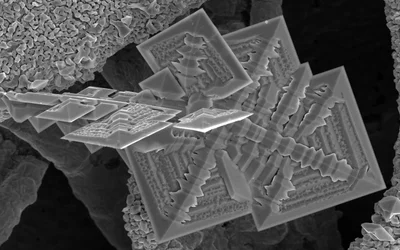
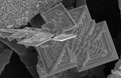
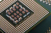
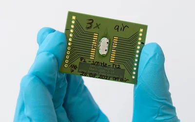
Semiconductors are the building blocks of modern electronics, powering everything from smartphones to satellites. This in-depth guide provides a comprehensive understanding of semiconductors' engineering principles and applications, delving into their fundamental concepts, materials, devices, manufacturing processes, and their impact on today's technology landscape.
Protect sensitive electronics by understanding the current limiting resistor, learning how to calculate appropriate values, and applying them in LEDs, transistors, microcontroller inputs and other circuits.
This guide explains how potentiometer pins interact with mechanical rotation, resistive tracks, and load conditions across various circuit configurations. It provides clarity for both low-power electronic designs and high-precision embedded systems.
This technical article explains the theory behind potentiometer schematics. It shows how to implement mechanical and digital potentiometers in practical circuits, tailored for engineers, and students.
Engineering teams can achieve AI-ready design data with five-level maturity model by Keysight. The unified, traceable data accelerates design cycles, boosts IP reuse, and reduces costly re-spins.
Source transformation is the method of converting a voltage source with series resistance into an equivalent current source with parallel resistance (and vice versa). This guide explains the theory, math, circuit examples, and practical applications for modern digital and hardware engineers.
Resistors are the quiet regulators of electronic circuits. They shape current, set voltages, bias transistors, protect components, and stabilize signals. This article breaks down the physics of resistance, explores modern resistor technologies, and offers practical guidance.
Many beginners may be confused about the Solder Mask Layer and Paste Mask Layer because they share some similarities. In this article, we will introduce the differences between solder masks and paste masks, enabling beginners to gain a better understanding.
Ground is the reference point that makes voltage meaningful and the return path that allows current to flow. This article explains what is ground in a circuit, discusses different types of grounds, and shows how to implement effective grounding strategies
Additive electronics is intrinsically more sustainable than subtractive processes. Yet the current materials are often based on metallic inks and plastic substrates. This is a particular issue in medical wearables with disposable devices. Hence the need to develop sustainable material options
An In-depth Analysis of Features, Applications, and Selection Criteria for Embedded Systems Design. Discover the Advantages and Limitations of SPI, I2C, and UART for Efficient Data Exchange in Various Scenarios.
Integrated photonics, also known as planar lightwave circuits or integrated optical circuits, revolutionizes optical communication by leveraging the properties of light to process and transmit information. This cutting-edge technology offers superior efficiency and compactness compared to traditional electronic components, paving the way for faster and more energy-efficient communication systems. With its interdisciplinary nature encompassing materials science, quantum physics, and electrical engineering, integrated photonics presents an exciting and promising field of study and research in today's digital era.
Advanced testing methodologies and innovation in semiconductor packaging ensure product reliability in dynamic and harsh operational environments. These strategies are particularly crucial in the rapidly evolving automotive industry.
A guide to resources related to the Nordic Semiconductor nRF9160 Development Kit and Soracom connectivity to help you launch your Connect For Good Low Power Wireless Sustainability Challenge submission.
Mesh topology is the most used network topology, as all computer networks are connected. Each computer sends signals and relays the data from other computer networks. The dedicated link transmits information from one node to another and connects all the nodes.
2D and 3D Automated inspection systems are often used for detecting manufacturing errors in fast production lines. Learn how they provide a comprehensive and efficient solution for quality assurance.
With the increasing need for critical applications technology, PCBAs have become smaller and more complex, requiring designers to create more individual designs in a shorter timeframe. Learn how to do so while avoiding common errors that can derail your project.
Mass manufacturing electronic textiles and in doing so combining textile based wiring and sensors with PCB electronics is no easy task. In this article, you will learn about an innovative approach to enable embriodery of PCBs and conductive wiring/sensors in mass produced e-textiles
Silicon, with its abundant availability and unique properties, serves as the fundamental building block for semiconductor manufacturing. Its semi-metallic nature makes it an ideal material for controlled conduction of electricity. Furthermore, the combination of silicon with oxygen produces silicon dioxide, a crucial insulating component in silicon chip manufacturing.
Die attach, also known as die bonding or die mount, is a process used in the semiconductor industry to attach a silicon chip to the die pad of a semiconductor package's support structure, such as a leadframe or metal can header. This article explores the fundamentals of die attach, its importance, materials, and methods used in die attach, its parameters, quality, and reliability techniques.