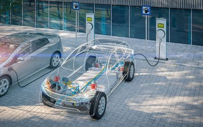
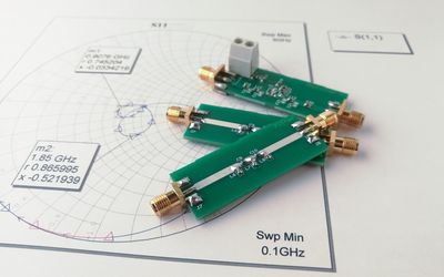
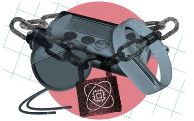
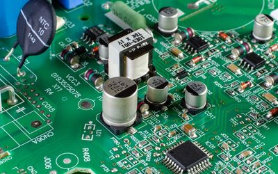
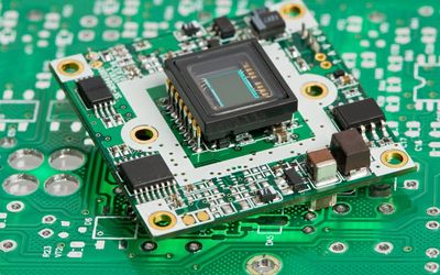
Be the first to know.
Get our Electronics  weekly email digest.

Electronics

report

The Guide to Understanding the Technologies Defining the Next Phase of Edge AI

PCB Trace Width Calculator

Featured

Wearable electronic textiles are a demanding environment for reliable interconnects – the ability to function with movement and survive multiple cleanings and reuse. Good adhesion is particularly challenging in these wearable and conformable electronics applications. While solders provide the most conductive electrical connection, they are rigid and require not only the addition of an underfill adhesive but usually a post bond encapsulation. This Anisotropic Conductive Epoxy, provides reliable interconnections between electronic components and circuitry on textiles with excellent structural bonding, without encapsulation, even under repeated stretching and washings. This technology has been shown as a scalable assembly process for e-Textile manufacturing in an SMT line.

Reliable, Scalable, Anisotropic Interconnect Solution for Wearable Electronics
Featured

Wafer thinning is a part of the semiconductor manufacturing process. It is essentially grinding off the backside of the wafers to control their thickness and is useful for the production of ultra-thin wafers. These flattened wafers are used to effect stacked and high-density packaging in compact or microelectronic devices. This article discusses the meaning of wafer thinning, along with its various techniques and significance.

Wafer Thinning: Investigating an essential part of semiconductor fabrication

Engineers Wiki. Most Asked Questions.

This article explains the IPC-A-610 standard for electronic assemblies, including solder joints, inspection criteria, product classes, and quality requirements for reliable PCB manufacturing and high-performance electronics.

ORGANIZATIONS. SHAPING THE INDUSTRY.

Mouser Electronics

Electronics

Mouser Electronics is a worldwide leading authorized distributor of semiconductors and electronic components.

219 Posts

MacroFab

EMS manufacturing

A better way to build electronics through a redefined experience, innovativ...

79 Posts

TechBlick

Electronics

TechBlick is a year round platform for onsite and online conferences, class...

65 Posts

Xsens

Appliances, Electrical, and Electronics Manufacturing

Xsens digitizes movement.

47 Posts

Murata Electronics

Electrical and Electronics Manufacturing

Join the Innovators in Electronics.

37 Posts

TAGGED WITH microchips

Latest Posts

Wearable electronic textiles are a demanding environment for reliable interconnects – the ability to function with movement and survive multiple cleanings and reuse. Good adhesion is particularly challenging in these wearable and conformable electronics applications. While solders provide the most conductive electrical connection, they are rigid and require not only the addition of an underfill adhesive but usually a post bond encapsulation. This Anisotropic Conductive Epoxy, provides reliable interconnections between electronic components and circuitry on textiles with excellent structural bonding, without encapsulation, even under repeated stretching and washings. This technology has been shown as a scalable assembly process for e-Textile manufacturing in an SMT line.

Reliable, Scalable, Anisotropic Interconnect Solution for Wearable Electronics

Wafer thinning is a part of the semiconductor manufacturing process. It is essentially grinding off the backside of the wafers to control their thickness and is useful for the production of ultra-thin wafers. These flattened wafers are used to effect stacked and high-density packaging in compact or microelectronic devices. This article discusses the meaning of wafer thinning, along with its various techniques and significance.

Wafer Thinning: Investigating an essential part of semiconductor fabrication

This article describes the TAeTTOOz printable battery technology developed by Evonik and acquired by InnovationLab for upscaling and mass production. In this article, you can learn about the operating principles, the key working characteristics, the material set, production techniques, and emerging applications of this technology

How rechargable disposable thin printed batteries can be produced and used to reliability power IoT products?

The progress of screen printing towards fine line printing has been incredible going from 100 µm features before 2010 to 70 µm to 2015 to 40 µm in 2018 and now pushing - in development- towards 20 µm and less. In parallel, the wet thickness of the printed line have gone down from 12um or so in 2018 to now just 4um.

The three themes are closely linked since QDs can be digitally printed as color conversation materials atop blue microLEDs to enable wide color gamut RGB uLED displays without requiring a separate transfer step for each color.. This is an important technology as it simplifies the manufacturing step for microLED and thus removing a major hinderence.

PCB layers are the copper layers within a printed circuit board, laminated between or onto layers of conductive material. These layers are stacked to enhance the functionality of electronic devices. This article explores the concept of PCB layering, the various types of layers, and their benefits.

PCB Layers: Everything You Need to Know