Featured

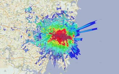
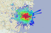
A new study suggests mobile data collected while traveling over bridges could help evaluate their integrity.

This guide is written for engineers and technical teams building connected devices who need clear, field-ready guidance without getting lost in standards documentation.
PCB Trace Width Calculator
A new study suggests mobile data collected while traveling over bridges could help evaluate their integrity.
Human activity, from climate change, pollution, and habitat destruction, to poaching, territorial conflict, and trophy hunting, has seen the IUCN’s list of endangered species balloon to more than 147,000 in recent years, with 41,000 species threatened with extinction.
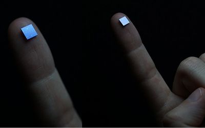
A unique new approach of printing functional materials with unparallel precision and repeatability. Technology called Ultra-Precise Deposition (UPD) is a nanodispensing method capable to print high density and high viscous materials with the resolution down to 1 µm in feature size and with high ratio of width to height after single pass. For this method material extrusion is controlled by a pressure, which means it is not supported with high electric field. Thanks to this there are no limitation if the substrate is conductive or dielectric.
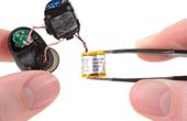
Understanding the key differences between the two high-in-demand battery types. This article focuses on Energy density, lifespan, safety, and cost trade-offs for the technical selection of Li-Ion and LiFePO4 batteries.
16 minutes read.
20 minutes read.
15 minutes read.
20 minutes read.
13 minutes read.
28 minutes read.


Electronics
Mouser Electronics is a worldwide leading authorized distributor of semiconductors and electronic components.
219 Posts
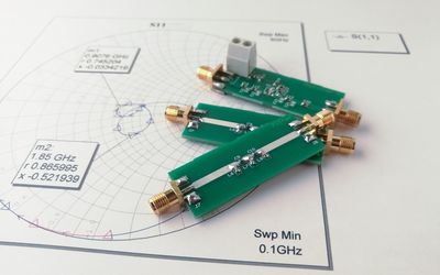
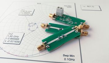
A guide covering the full radio-frequency design workflow, starting from setting specifications and choosing topologies to matching, simulation, layout, and verification, to help antenna engineers.
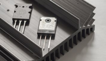
This article presents a detailed technical exploration of SiC MOSFET devices, covering material physics, device structure, switching behavior, and practical design considerations for high-efficiency power electronics systems.
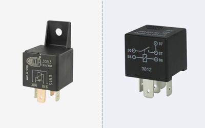
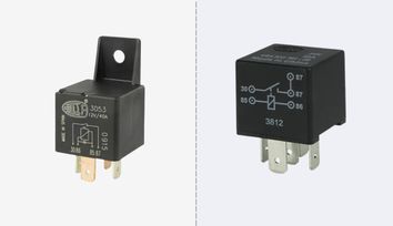
This article is a comprehensive technical guide to relay wiring diagrams, covering 4-pin and 5-pin configurations, working principles, safety practices, standards, and advanced relay applications in modern systems.
Explore how frequency shapes EMC behavior from RF emissions to ultra-low-frequency drift, with mitigation strategies for robust, compliant electronic system design.
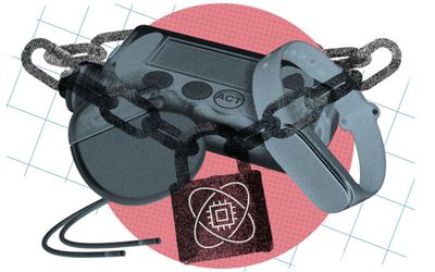
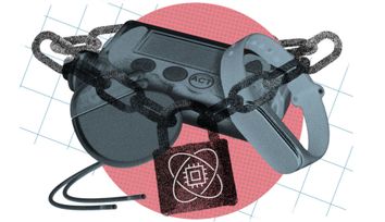
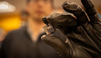
Ultra-efficient chip design enables extremely strong cryptography algorithms to run on energy-constrained edge devices.
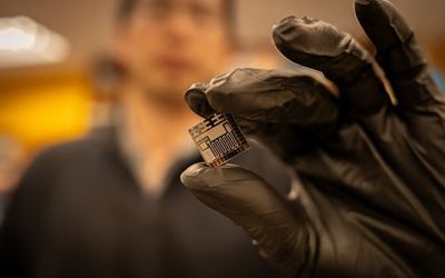
Researchers at ETH Zurich have now developed chip technology that enables verification of the authenticity of sensor data, including images or videos.
The integrated design achieves accurate micro gas chromatography and can help reduce the cost of monitoring chemical synthesis, natural gas pipelines or at-home air quality.
Hybrid bonding provides the adhesive free, copper to copper interconnects that are driving cutting edge 3D chip stacking. This article explains the theory, process, benefits, challenges, applications, and emerging trends of hybrid bonding for engineers.
A new study suggests mobile data collected while traveling over bridges could help evaluate their integrity.
Human activity, from climate change, pollution, and habitat destruction, to poaching, territorial conflict, and trophy hunting, has seen the IUCN’s list of endangered species balloon to more than 147,000 in recent years, with 41,000 species threatened with extinction.

4 minutes read
A unique new approach of printing functional materials with unparallel precision and repeatability. Technology called Ultra-Precise Deposition (UPD) is a nanodispensing method capable to print high density and high viscous materials with the resolution down to 1 µm in feature size and with high ratio of width to height after single pass. For this method material extrusion is controlled by a pressure, which means it is not supported with high electric field. Thanks to this there are no limitation if the substrate is conductive or dielectric.

2 minutes read
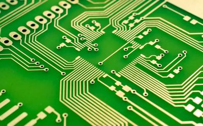
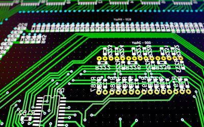
PCB traces are fundamental components in circuit design, serving as the pathways for electrical signals. This article examines the advancements, applications, and challenges of PCB trace technology. Discover insights into optimizing designs and overcoming common obstacles in PCB trace implementation.
With some foresight, most CAD design layout packages can accommodate castellated edge designs.

3 minutes read
Using Artificial Intelligence (AI) to replace optical and mechanical components, researchers have designed a tiny spectrometer that breaks all current resolution records.
Bringing a product to market late has a real and negative impact on profits and brand reputation. In this blog, we go through the types of documentation your project requires and ways to streamline processes.
3 minutes read
Using a new technology, researchers hope to create better control systems for prosthetic limbs.
This article delves into the core variations between PMOS and NMOS, exploring their fundamentals, structural differences, operating principles, and practical applications.
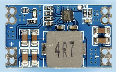
Article #8 of Power Management for Tomorrow’s Innovations Series: Power electronics converters with an efficiency of up to 95% and very low quiescent current can make the Internet of Things devices last for months together.
Article #7 of Power Management for Tomorrow’s Innovations Series: Power supplies utilized in the medical industry must be compact, reliable, long-lasting, and robust.
Article #6 of Power Management for Tomorrow’s Innovations Series: Power supplies for vehicle asset-tracking devices must be designed to operate at different voltage-current levels, be compact, and offer protection during transients and electrical faults.
Article #5 of Power Management for Tomorrow’s Innovations Series: Single-Inductor Multiple-Output (SIMO) architecture enables design engineers to extend the battery life, and reduce the circuit board size for hearables and wearables
Article #4 of Power Management for Tomorrow’s Innovations Series: This article investigates the effect that power designs have on the phase noise of Radio Frequency amplifiers through an experiment comparing the performance of three power regulators at different frequencies.
Article #3 of Power Management for Tomorrow’s Innovations Series: Digital Power System Managers facilitate accurate measurement of the output current to let power supplies operate reliably and offer protection in case of electrical faults.