Featured
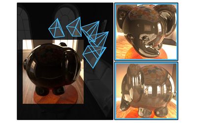
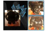
A new computer vision system turns any shiny object into a camera of sorts, enabling an observer to see around corners or beyond obstructions.

This guide is written for engineers and technical teams building connected devices who need clear, field-ready guidance without getting lost in standards documentation.
PCB Trace Width Calculator
A new computer vision system turns any shiny object into a camera of sorts, enabling an observer to see around corners or beyond obstructions.
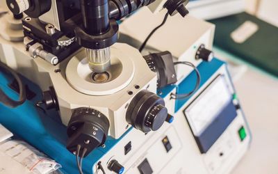
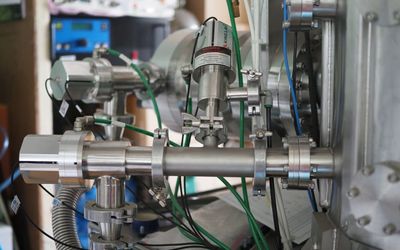
Ion milling is a material etching technique used extensively in modern manufacturing and research. It involves the bombardment of a sample with charged particles, called ions, to remove material from the surface in a controlled manner. This article explores the fundamental principles of ion milling, the various techniques used, the equipment required, and its applications in different fields.
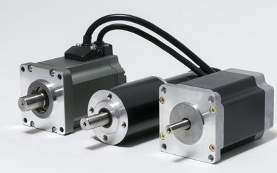
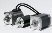
In this article, we will delve into the key factors that differentiate stepper and servo motors, including their operating principles, torque characteristics, control methods, and suitability for different applications.
Understanding the key differences between the two high-in-demand battery types. This article focuses on Energy density, lifespan, safety, and cost trade-offs for the technical selection of Li-Ion and LiFePO4 batteries.
16 minutes read.
20 minutes read.
15 minutes read.
20 minutes read.
13 minutes read.
28 minutes read.

Electronics
Mouser Electronics is a worldwide leading authorized distributor of semiconductors and electronic components.
219 Posts
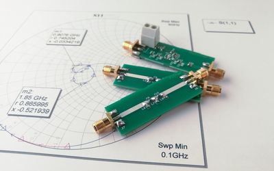
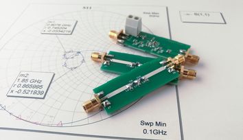
A guide covering the full radio-frequency design workflow, starting from setting specifications and choosing topologies to matching, simulation, layout, and verification, to help antenna engineers.
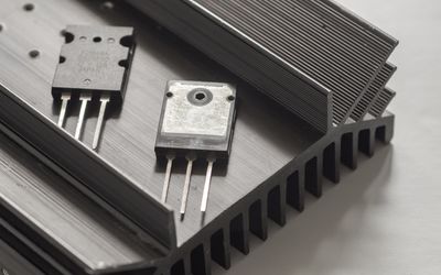
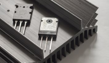
This article presents a detailed technical exploration of SiC MOSFET devices, covering material physics, device structure, switching behavior, and practical design considerations for high-efficiency power electronics systems.
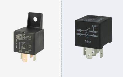
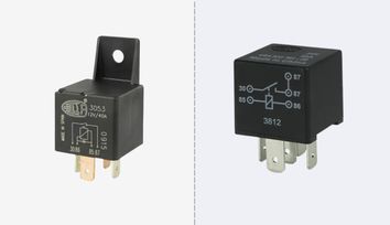
This article is a comprehensive technical guide to relay wiring diagrams, covering 4-pin and 5-pin configurations, working principles, safety practices, standards, and advanced relay applications in modern systems.
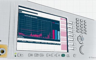
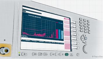
Explore how frequency shapes EMC behavior from RF emissions to ultra-low-frequency drift, with mitigation strategies for robust, compliant electronic system design.
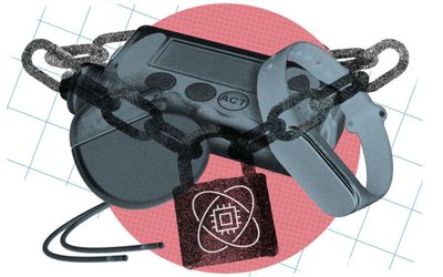
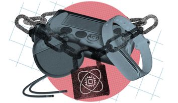
Ultra-efficient chip design enables extremely strong cryptography algorithms to run on energy-constrained edge devices.
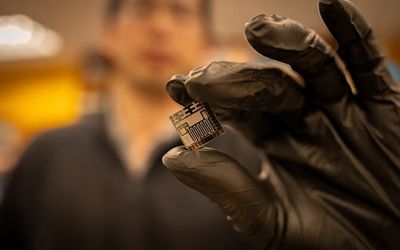
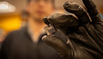
Researchers at ETH Zurich have now developed chip technology that enables verification of the authenticity of sensor data, including images or videos.
The integrated design achieves accurate micro gas chromatography and can help reduce the cost of monitoring chemical synthesis, natural gas pipelines or at-home air quality.
Hybrid bonding provides the adhesive free, copper to copper interconnects that are driving cutting edge 3D chip stacking. This article explains the theory, process, benefits, challenges, applications, and emerging trends of hybrid bonding for engineers.
A new computer vision system turns any shiny object into a camera of sorts, enabling an observer to see around corners or beyond obstructions.
Ion milling is a material etching technique used extensively in modern manufacturing and research. It involves the bombardment of a sample with charged particles, called ions, to remove material from the surface in a controlled manner. This article explores the fundamental principles of ion milling, the various techniques used, the equipment required, and its applications in different fields.
In this article, we will delve into the key factors that differentiate stepper and servo motors, including their operating principles, torque characteristics, control methods, and suitability for different applications.
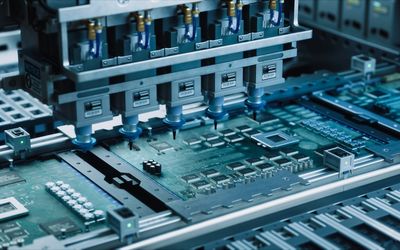
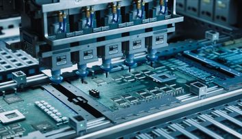
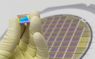
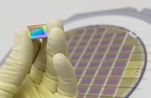
Wafer dicing separates individual integrated circuits or chips from a semiconductor wafer without damaging their delicate structures and circuits. This process is crucial for the production of electronic devices and components used in various industries, and the demand for it has increased with the development of high-performance and smaller electronic devices. Different dicing techniques, such as blade dicing, laser dicing, and plasma dicing, have been developed, and new innovations continue to emerge to address the challenges of complex semiconductor devices.
Learn the powerful approach of combining data from multiple sensors to enhance the overall perception, reliability, and decision-making capabilities of various systems with ease.
An Overview of Magnetron Sputtering and its Applications in Thin Film Growth
In this article, we will delve into the structure and operation of NMOS and PMOS transistors, and discuss the applications and characteristics of these essential components in electronic circuits.
Article #1 of Transforming Industrial Manufacturing with Industry 4.0 Series: Advancements in less-glamorized technologies like sensing, Programmable Logic Controllers, low-power components, and vision systems have played important roles in the rapid progression of Manufacturing 4.0.
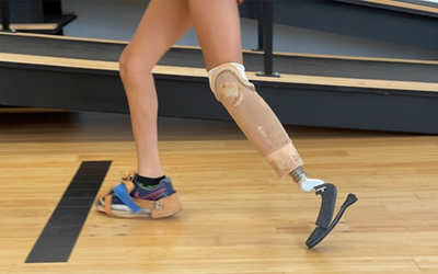
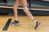
Research from elite athletes informs the design of these robust and adaptable prosthetics. We interview researcher Tijmen Seignette, about his ambitions to change how we approach prosthetic design.
Columbia Engineers design a robot hand that is the first device of its kind to join advanced sense of touch with motor-learning algorithms — it doesn’t rely on vision to manipulate objects
A new low-temperature growth and fabrication technology allows the integration of 2D materials directly onto a silicon circuit, which could lead to denser and more powerful chips.
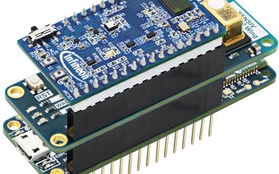
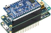
How plug-and-play IoT sensor platforms can speed up product development
This free-to-attend, immersive virtual event, on 22 June 2023 will cover all aspects of flexible and printed electronics, from material advancements to the development of novel deposition and manufacturing technologies.
In today's interconnected world, network topologies play a crucial role in determining the efficiency and reliability of communication between devices. One such network topology is the bus topology, known for its simplicity and cost-effectiveness. In this comprehensive guide, we will delve deeper into bus topology, exploring its advantages, disadvantages, applications, and the future of this network design.
Meet the ten finalists of the ROCK Engineering Challenge and vote for your favorite.