
Featuredcase study
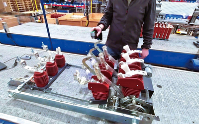
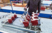
ABB Poland streamlined switch inspection with SCANTECH's SIMSCAN-E 3D scanner, enabling fast, accurate, spray-free scanning of reflective components, and accelerating both quality control and reverse engineering processes.
The Guide to Understanding the Technologies Defining the Next Phase of Edge AI
PCB Trace Width Calculator
ABB Poland streamlined switch inspection with SCANTECH's SIMSCAN-E 3D scanner, enabling fast, accurate, spray-free scanning of reflective components, and accelerating both quality control and reverse engineering processes.
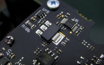
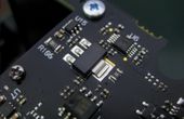
Reliable connections are critical in cutting-edge medical devices.
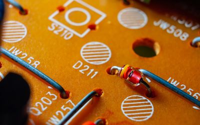
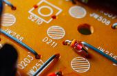
Zener diodes are unique semiconductor devices designed to operate in reverse bias and maintain a stable voltage. This article explains how a Zener diode works, from its quantum-tunneling breakdown mechanism to practical uses in voltage regulation and circuit protection.
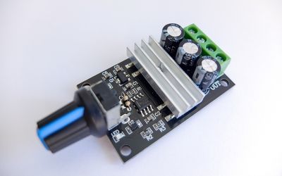
This article explains practical DC motor speed control techniques for both brushed and BLDC systems, covering design principles, control methods, and engineering considerations behind reliable motor speed control.
20 minutes read.
15 minutes read.
20 minutes read.
13 minutes read.
28 minutes read.


Electronics
Mouser Electronics is a worldwide leading authorized distributor of semiconductors and electronic components.
219 Posts
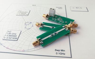
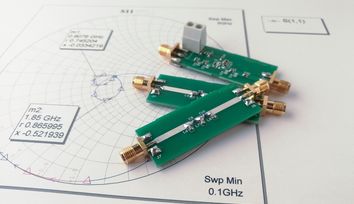
A guide covering the full radio-frequency design workflow, starting from setting specifications and choosing topologies to matching, simulation, layout, and verification, to help antenna engineers.
This article presents a detailed technical exploration of SiC MOSFET devices, covering material physics, device structure, switching behavior, and practical design considerations for high-efficiency power electronics systems.
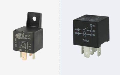
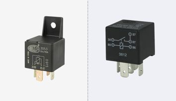
This article is a comprehensive technical guide to relay wiring diagrams, covering 4-pin and 5-pin configurations, working principles, safety practices, standards, and advanced relay applications in modern systems.
Explore how frequency shapes EMC behavior from RF emissions to ultra-low-frequency drift, with mitigation strategies for robust, compliant electronic system design.
Ultra-efficient chip design enables extremely strong cryptography algorithms to run on energy-constrained edge devices.
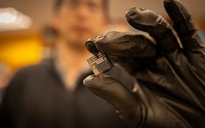
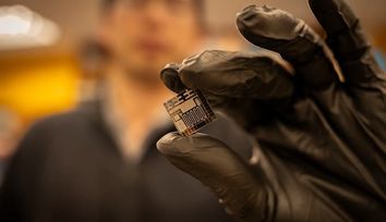
Researchers at ETH Zurich have now developed chip technology that enables verification of the authenticity of sensor data, including images or videos.
The integrated design achieves accurate micro gas chromatography and can help reduce the cost of monitoring chemical synthesis, natural gas pipelines or at-home air quality.
Hybrid bonding provides the adhesive free, copper to copper interconnects that are driving cutting edge 3D chip stacking. This article explains the theory, process, benefits, challenges, applications, and emerging trends of hybrid bonding for engineers.
ABB Poland streamlined switch inspection with SCANTECH's SIMSCAN-E 3D scanner, enabling fast, accurate, spray-free scanning of reflective components, and accelerating both quality control and reverse engineering processes.

3 minutes read
Reliable connections are critical in cutting-edge medical devices.
Zener diodes are unique semiconductor devices designed to operate in reverse bias and maintain a stable voltage. This article explains how a Zener diode works, from its quantum-tunneling breakdown mechanism to practical uses in voltage regulation and circuit protection.
In this article, we will provide a brief overview of fluid dispensing systems, highlight their applications, discuss common challenges with the technology, and share an overview of NOVA, our materials dispensing system.

5 minutes read
Article #5 of Confronting AI Series: Smart ML on embedded systems demands efficiency under tight memory, compute, and latency constraints. Techniques like pruning, quantization, low-rank decomposition, and federated learning enable compact, fast, and reliable models for edge intelligence.
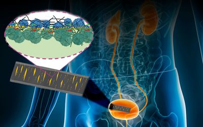
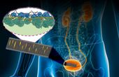
A new skin-like sensor developed by an international team led by researchers at Penn State could help doctors monitor vital signs more accurately, track healing after surgery and even help patients with bladder control issues.
Learn the step-by-step process of testing MOSFET transistors using a digital multimeter and simple circuits. This comprehensive guide covers MOSFET fundamentals, diagnostic techniques, and practical tips for engineers and electronics students.
Vision-driven, multi-arm robotics are set to transform the factory itself into a configurable product, capable of switching from one assembly task to the next with a software update instead of a hardware rebuild. Learn more now in our latest report.
A once-overlooked technology that taps into the Earth's heat to generate electricity could supply up to 20% of the electricity in the United States by 2050, according to a new Princeton analysis.

4 minutes read
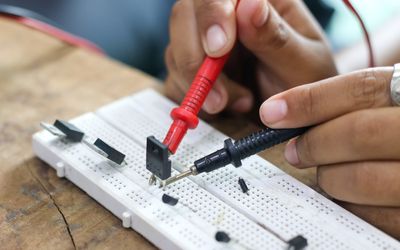
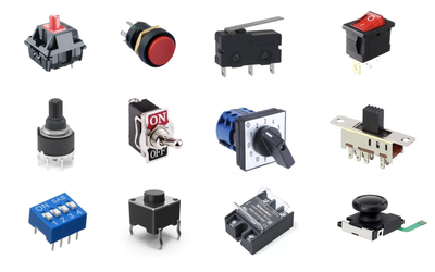
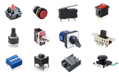
This technical guide details various types of switches, highlighting their configurations, functionality, emerging technologies, and selection criteria for choosing a right one for your application!
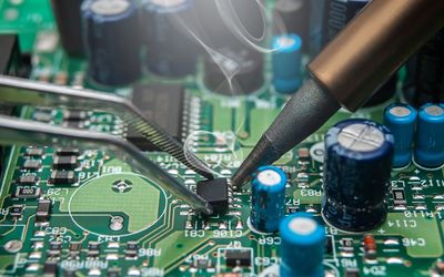
Desoldering is the process of removing solder to detach components from a PCB. Whether you're repairing hardware, modifying a design, or salvaging parts, this hands-on guide walks you through the tools, techniques, and safety tips every electronics pro needs.
Master circuit grounding fundamentals, from voltage references to EMI control, with practical implementation strategies for modern electronics design.
Thin electrode arrays integrate seamlessly into developing embryos' brains

3 minutes read
How do MOSFETs work? This article provides an in-depth exploration of their internal structure, electrical characteristics, operation modes, real-world use cases, and the latest technological advancements and trends for 2025!
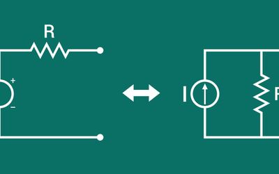
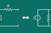
Learn how source transformation simplifies complex circuit analysis by converting between Thévenin voltage sources and Norton current sources – complete with definitions, derivations, step-by-step examples (including dependent and AC sources), common pitfalls, and advanced applications.