How to Test a Circuit Board (PCB): Methods, Tools, and Best Practices
PCB testing verifies the structural integrity and performance of a circuit board. This article explores key insights from design for testability (DFT) to manual and automated tests such as AOI, ICT, and X-ray.

30 May, 2025. 29 minutes read
Introduction
When you assemble a new printed circuit board (PCB), the real test begins when you power it up—an event engineers jokingly call it “smoke test.” If something’s gone wrong, you might literally see smoke, indicating a serious design or manufacturing flaw. That’s why PCB testing is such a critical step in electronics development. Whether you're a hardware engineer, digital design expert, or electronics student, understanding how to test a PCB is essential for ensuring reliability and preventing costly failures.
PCB testing involves verifying both the structural integrity and functional performance of a board. In simpler terms, it checks whether the board was built correctly—free from defects like solder bridges, broken traces, or misaligned components—and confirms that the circuit behaves exactly as it was designed to.
Theoretical Concepts Behind Circuit Board Testing
At its core, PCB testing is about answering two critical questions: Was the board built correctly? And does it function as intended? Given the complexity of modern printed circuit boards—with their dense arrangements of components, multilayer traces, and precise electrical characteristics—even a small defect can lead to complete failure. Testing aims to uncover two types of problems: manufacturing defects like solder bridges, missing or misaligned components, and design issues such as incorrect circuitry behavior. Common faults include short circuits (unintended connections), open circuits (broken or unconnected traces), wrong or reversed components (e.g., flipped ICs or diodes), and incorrect component values. These issues can cause a board to fail, behave erratically, or only break down under specific conditions, making early detection essential.
PCB testing methods fall into two main categories: structural testing and functional testing. Structural tests (often called in-circuit or electrical tests) assess the physical and electrical correctness of the assembled board without applying full operational power. These tests verify that all required connections exist (no opens), there are no unwanted connections (no shorts), and each component is correctly placed and electrically accurate. Techniques include resistance and capacitance measurements, Automated Optical Inspection (AOI), and X-ray imaging to find hidden solder issues. For instance, an in-circuit test can measure a resistor’s value or check the polarity of a diode to ensure correct placement, catching faults early before the board is powered up.
In contrast, functional testing evaluates the PCB’s behavior under real operating conditions. This involves powering the board—sometimes carefully at first—and verifying that it performs its intended functions. It can range from simple “smoke tests” (to check for catastrophic faults) to comprehensive diagnostic routines, such as applying known signals to inputs and checking outputs, or running embedded firmware to validate microcontroller performance. Functional testing mimics how the board will operate in the field, ensuring that timing, logic, and performance meet specifications.
To maximize test effectiveness, engineers aim for high fault coverage—the percentage of possible faults that can be detected. No single test method can catch all errors, so combining approaches is standard practice. For example, AOI can catch visual flaws like tombstoned capacitors or cold solder joints, while electrical tests detect invisible problems like an open via. Functional tests, on the other hand, confirm that everything works together as intended.
Another essential principle is Design for Testability (DFT). DFT involves adding features during the design phase to simplify testing later. Examples include adding test points to critical nets, using breakout headers, or routing signals in a way that allows easier probing. DFT doesn’t just make testing more accurate—it also reduces the time and cost of debugging.
In short, PCB testing is the structured effort to ensure “we built it right” through structural tests and “it works right” through functional tests. By understanding these foundational concepts, engineers can design and validate robust, reliable boards—well before a single spark flies.
Recommended reading: Mastering PCB Testing: Techniques, Methods, and Best Practices Unveiled
Pre-Test Design Considerations (Design for Testability)
Effective circuit board testing doesn’t begin after fabrication—it starts at the design stage. This forward-thinking approach, known as Design for Testability (DFT), involves integrating test-friendly features into the layout before the first trace is drawn or the component is placed.
By planning for testability early, engineers ensure that production testing, debugging, and validation are not only more efficient and comprehensive but also cost-effective. DFT helps detect faults faster, isolate issues with precision, and avoid costly rework due to hidden defects that standard testing might miss.
DFT isn’t just about making testing possible—it’s about making it practical. It prevents scenarios where a board passes most checks but fails in the one area that couldn’t be easily tested, leading to failures in the field.
Here are key DFT considerations before you even fabricate the PCB:
Incorporate Test Access Points for Effective PCB Testing
One of the foundational principles of Design for Testability (DFT) in PCB design is the inclusion of test access points, designated pads or vias that allow direct electrical access to critical nets on the board. These test points are essential for enabling automated or manual test equipment, such as oscilloscopes, multimeters, or in-circuit testers (ICT), to probe signals that might otherwise be inaccessible, especially those routed beneath components or buried in inner layers.
Strategically place test points on key signal paths, power rails, and ground planes. Each test pad should be large enough (typically 50–75 mils in diameter) and spaced sufficiently apart to accommodate testing fixtures like bed-of-nails or flying probe systems without causing mechanical interference or electrical shorts. Avoid clustering test points too closely, as this can hinder probe access and increase the risk of crosstalk or unintended shorts.
To optimize test efficiency, group related test points in accessible regions of the board layout, maintaining enough clearance for standard probe sizes. Including dedicated test pads for each power rail and for ground is particularly important; they not only simplify the connection of diagnostic tools but also help maintain stable signal references and reduce noise during testing.
Designing for In-Circuit Test (ICT) and Fixture Compatibility
When preparing a PCB for high-volume production, it's essential to design with In-Circuit Testing (ICT) in mind, particularly if a bed-of-nails fixture will be used. ICT relies on a dense array of spring-loaded pogo pins to make simultaneous contact with test points, so your PCB layout must support both mechanical and electrical access.
Key design considerations include:
Adequate Clearance Around Test Pads: Ensure each test pad has enough spacing to prevent mechanical interference between adjacent pogo pins and to avoid accidental shorts.
Height Restrictions: Avoid placing tall or bulky components near test areas, especially if they could obstruct the vertical access needed by the probes.
Uniform Test Point Distribution: Distribute test points evenly across the board. Concentrating them in a single region can increase fixture complexity and decrease test reliability.
Bottom-Side Accessibility: Most ICT fixtures are designed to probe the bottom side of the PCB. Therefore, unless otherwise specified by your manufacturer, place all test pads and tooling holes (for alignment and mounting) on that side.
Standard Grid Layout and Fiducials: Follow the manufacturer's ICT guidelines—this often includes maintaining a standard pad pitch (e.g., 100 mil grid) and adding fiducial markers for automated optical alignment during fixture setup.
Designing a board that supports ICT from the outset not only speeds up production-line testing but also enhances fault coverage and reduces overall testing costs. A well-planned ICT layout enables fast, parallel probing of multiple test nodes, ensuring robust quality control in mass manufacturing environments.
Expose Critical Nets and Leverage Existing Connectors for Testing
Beyond dedicated test pads, existing board connectors and headers can serve as valuable test access points. Signals routed to power, programming, or communication connectors can often be reused during testing to monitor or control the board without needing additional access points.
For instance:
Power and Programming Interfaces: Connectors used to deliver power or program firmware can also provide test access to key power rails or digital signals during bring-up and functional testing.
JTAG Headers: If your main ICs support boundary scan (e.g., via JTAG), consider including a JTAG header—even if it's not needed in the final product. It provides powerful capabilities for in-system debugging, interconnect testing, and even in-circuit programming.
Communication Ports: Interfaces like UART, USB, or SPI can be repurposed during functional testing for logging test data, issuing commands, or interacting with automated test software.
The overarching principle is to ensure that all critical signals and nodes—whether digital, analog, or power—are accessible for test and debug purposes. This flexibility can significantly simplify hardware validation, accelerate fault diagnosis, and reduce the need for physical rework or intrusive probing later in the process.
Implement Isolation Mechanisms and Test Modes
Designing a PCB with the ability to isolate sections of the circuit or enter specific test modes is crucial for effective debugging and in-circuit testing (ICT). These features allow individual components or subsystems to be evaluated independently, making it easier to pinpoint issues and verify functionality during bring-up or automated testing.
Key techniques include:
Jumpers, DIP Switches, or Configurable Resistors: These can be used to electrically disconnect specific sections of the board, such as sensors, power drivers, or communication modules, during early testing. This allows you to verify fundamental circuits (e.g., power regulation, microcontroller operation) before enabling more complex or high-power elements.
Forced Reset or Tri-State Control: Incorporate pull-up or pull-down resistors, or control signals via jumpers or test pins, to hold certain ICs in a disabled state (e.g., reset or high-impedance output). This prevents them from driving signals or drawing current that could interfere with in-circuit measurements of other components.
Clock Override Options: Provide test points or control logic that allow clock sources (e.g., crystal oscillators or PLLs) to be disabled or overridden during testing. This is especially useful when testing logic that is clock-dependent, as it allows you to control timing or isolate potential issues related to signal synchronization.
By building in isolation and test configurations from the design phase, you give test engineers the ability to validate each part of the system independently. This improves fault visibility, simplifies troubleshooting, and prevents system-level behavior from masking localized faults—ultimately enhancing test coverage and reducing debug time.
Label and Document All Test Points Clearly
While often overlooked, clear labeling and thorough documentation of test points are essential best practices in PCB design for testability. Each test pad, jumper, or configuration pin should be distinctly labeled on the silkscreen—using consistent naming conventions such as TP1, TP2, or descriptive names like BOOT_EN, RESET_SEL, etc.
In addition to on-board labeling, create a detailed test point map in your design documentation. This should include:
Reference Designators (e.g., TP1, JP3)
Net Names (e.g., VCC_3V3, UART_TX, I2C_SCL)
Coordinates or Physical Locations
Intended Use (e.g., power measurement, firmware debug, reset control)
This documentation enables faster manual probing during troubleshooting, reduces guesswork during bring-up, and streamlines the design of ICT or flying probe test fixtures. With accurate silkscreen labels and a well-maintained signal map, test engineers can immediately identify where to place probes or connect test equipment, saving time, minimizing errors, and improving test efficiency throughout development and production.
Utilize Built-In Self-Test (BIST) and Diagnostic Firmware
For systems incorporating complex ICs, such as microcontrollers, SoCs, or FPGAs, leveraging built-in self-test (BIST) capabilities can significantly enhance your overall test strategy. Many of these devices include internal mechanisms to verify memory integrity, peripheral functionality, or internal logic blocks.
To maximize this advantage:
Integrate a Manufacturing Test Mode: Design your firmware to include a dedicated test mode that runs upon command or under specific conditions. This mode can perform automated checks on RAM, flash, GPIOs, communication interfaces (e.g., UART, I2C, SPI), user input devices, and LEDs.
Enable Diagnostic Output: Allow the test firmware to report results through serial ports, USB interfaces, or even via simple LED blink codes. This makes it easy to interpret pass/fail results during production or bring-up without requiring complex external equipment.
Modularize the Test Software: Structure your code so that test routines can be run independently from the main application. This not only improves maintainability but also allows selective testing during different stages of the development or production cycle.
While BIST is primarily a software consideration, it plays a critical role in Design for Testability (DFT) from a system perspective. By planning and integrating diagnostic features into both the hardware and firmware, you enable faster fault isolation, reduce reliance on external test equipment, and streamline validation across the product lifecycle.
Recommended reading: What Is In-Circuit Testing? An Essential Guide for Engineers
Manual Testing Methods (Visual Inspection, Continuity, Probing)
Before employing fancy equipment, start with the basics. Manual testing methods are the first line of defense in catching issues on a circuit board. These methods rely on the engineer’s observation and basic instruments (like a multimeter or oscilloscope) to verify the board. They are especially crucial during initial prototyping and bring-up, when you might not have automated test results yet. Let’s go through the key manual testing techniques: visual inspection, continuity and basic electrical checks, and probing with instruments.
Visual Inspection
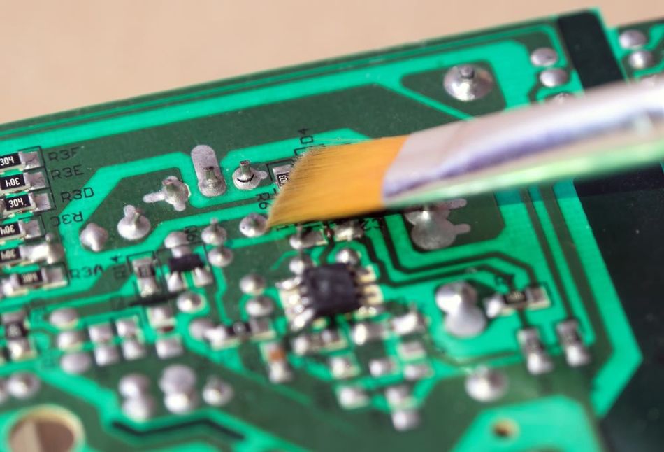
After a board is assembled (either by hand or by a manufacturer), visual inspection is a simple but powerful step. Under good lighting (and perhaps with a magnifier or microscope for fine-pitch components), scan the entire board for obvious problems. What to look for? Here’s a checklist:
Soldering issues: Are there any solder bridges (shorts) between pads, especially on IC pins? Are all solder joints shiny and solid, with no cold solder joints or cracks? Look at BGAs (if you have them) for any sign of uneven solder (though many BGA defects won’t be visible, requiring X-ray or other methods later). For through-hole parts, ensure solder has flowed on both sides of the board.
Component placement and orientation: Check that every component is present and placed in the correct location. It’s common in prototypes to accidentally omit a part or place one in the wrong spot. Verify that polarized components (diodes, electrolytic capacitors, LEDs, ICs) are oriented correctly as per the silkscreen or design (e.g., the notch on an IC aligns with the PCB’s mark). A surprisingly large number of board issues come down to “oops, that chip is rotated 90° off” – visual inspection will catch that. Also, confirm switch settings or jumper positions, if any, per the intended configuration.
Component values (visually): You can sometimes verify resistor values by their color codes or labels, and capacitor values if they are labeled. Check reference designators if visible, to ensure the right value is in the right place (for example, that a 10k resistor wasn’t accidentally soldered where a 100Ω should be). This may be hard to do for all parts without cross-referencing the BOM, but a quick glance might reveal an obviously wrong component (such as a large resistor where a tiny one should be, etc.).
Mechanical fit and connectors: See that the connectors (like USB ports, headers) are soldered straight and fully inserted. Ensure that any boards that plug into each other (if it’s a multi-board assembly) align correctly. Also check for foreign debris – occasionally a stray solder ball or screw could be lodged somewhere on the PCB, which could cause shorts.
Performing a thorough visual inspection can save you from powering on a board with a blatant short or missing component. It’s helpful to use a printed schematic or assembly drawing during inspection to cross-check each component and net. In professional settings, Automated Optical Inspection (AOI) machines do this type of check automatically (more on AOI later), but for a one-off board or prototype, manual inspection by the engineer is the way to go.
Recommended reading: PCB Inspection: Ensuring Quality and Reliability in Electronics Manufacturing
Continuity and Basic Electrical Checks
Once the board looks okay, the next step is to do some basic electrical tests before powering it up. The main tool here is a digital multimeter (DMM), used in continuity mode or resistance mode. Key checks include:
Power-to-Ground Shorts: Using the multimeter’s continuity buzzer or low-ohm measurement, check if any of the power rails are shorted to ground. Simply place one probe on a ground point and the other on each supply rail. Ideally, you should measure no short (infinite resistance). If the meter beeps or shows near 0Ω, that’s a red flag – there’s likely a solder bridge or misplaced component causing a short between that power net and ground (or between two power nets). It’s much better to find that now than by plugging in power and watching something burn. For multi-rail boards, check each voltage rail (5V, 3.3V, etc.) against ground. A reading of 0 volts or very low resistance where a voltage is expected means a probable short circuit on that rail.
Continuity of critical connections: You can also verify that certain important connections are made. For example, if you have a connector pin that should connect to a chip pin, you might test continuity between those points to confirm the trace is good (especially if you suspect a PCB fab issue or a via that might not be soldered). Also, check fuse continuity (if there’s an on-board fuse, ensure it shows near 0Ω as it should when intact).
Component value spot-checks: With the board unpowered, a multimeter can measure the resistance of resistors to ensure they are roughly the correct value (allowing for tolerance and parallel paths). For instance, you might measure a resistor and see ~10kΩ as expected. Be mindful that in-circuit measurements can be affected by other parallel components, so it might not read exactly the nominal value, but you can often catch gross errors (like a 0Ω where a 10kΩ should be, indicating a short or wrong component). Similarly, you can use the diode-test function of the DMM to check diode drops (ensuring diodes or transistor junctions are oriented properly by measuring the forward voltage). On simple boards, you can systematically check connections for opens/shorts by probing every net with the ohmmeter (a “buzz-out” test). On complex boards, that’s impractical manually, but you might still check a few key nets.
Insulation resistance between unrelated nets: This is a bit advanced, but if you suspect possible leakage or solder bridging, you can measure resistance between nets that should not connect (other than through high impedance). They should read as open (megaohms). Usually, this isn’t necessary unless you have reason to suspect an issue.
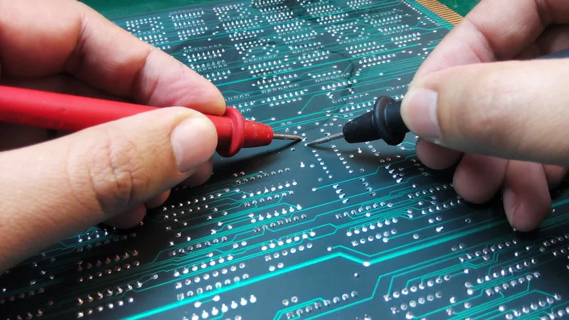
Probing with Oscilloscopes and Instruments
After confirming there are no shorts and everything is in place, it’s time for the initial power-on. It’s wise to use a bench power supply with current limiting for the first power-up. Set the supply to the correct voltage and a low current limit (just above what the board is expected to draw). This way, if there’s an unintended short, the supply will hit the current limit, and you won’t fry components immediately. This initial power application – the classic “smoke test” – should be done carefully while monitoring the board. If possible, touch (carefully) or use an infrared thermometer/camera to see if any component is unexpectedly heating up (a sign of a short or wrong connection). If something is heating or you smell smoke, cut the power and re-check for shorts or incorrect part orientation.
Assuming the power stays on and nothing catastrophic happens, you can proceed with measuring voltages on the board. Use the multimeter or an oscilloscope to check that all the power rails are at their expected voltages (within tolerance). This verifies that regulators are functioning and that no heavy loads are dragging down the supplies. If a rail measures significantly low or zero (and the supply is not current-limiting), that indicates a problem like a short or miswired regulator.
With the board powered, an oscilloscope becomes extremely useful for diagnostics. You can probe key signals to ensure they are present and within spec. For example, check the main clock oscillator output – is it oscillating at the correct frequency and amplitude? Probe reset lines to see if they are in the correct state (e.g., not stuck low). If the board has a microcontroller or FPGA, you might see if it’s driving any activity (some boards have status LEDs or test points you can monitor for digital activity). A logic analyzer can be employed to capture digital bus signals (like SPI, I²C, or parallel interfaces) once the system is running, to verify that communication is happening correctly.
During troubleshooting, use these instruments methodically. For instance, if part of the circuit isn’t working, probe at intermediate points to “divide and conquer.” Suppose an output is not coming on – check if the control signal into a MOSFET driver is present; if it is, then the problem might be the MOSFET or its connections. If it’s not, trace back to the microcontroller pin, and so on. By observing waveforms, you can detect issues like a signal stuck at high or low (could indicate a short to rail or a dead IC pin) or an unstable signal (could indicate oscillation or noise problems).
Automated Test Methods (ICT, Flying Probe, Boundary Scan, AOI, AXI)
While manual inspection and probing remain useful during early development and debugging, they fall short in high-volume production and for complex, densely packed PCBs. Manual methods are time-intensive, prone to oversight, and often incapable of detecting subtle or hidden defects. To overcome these challenges, automated testing methods are employed to enhance speed, accuracy, and test coverage in both prototyping and mass manufacturing environments.
The primary automated test technologies used in PCB manufacturing include:
In-Circuit Testing (ICT)
In-Circuit Testing (ICT) is a cornerstone of PCB validation in high-volume manufacturing. It’s a type of structural test that evaluates the electrical integrity of individual components and interconnections on an assembled PCB. ICT identifies manufacturing defects early in the production cycle, making it invaluable for ensuring quality and reliability before boards move further down the line.
How ICT Works
At the heart of ICT is a custom test fixture, commonly called a bed-of-nails, which houses hundreds—or even thousands—of spring-loaded pogo pins. These pins are precisely aligned to make contact with test points, vias, or component leads on the PCB when it is pressed into the fixture. This setup allows the tester to simultaneously access numerous nodes on the board and rapidly perform a comprehensive set of electrical tests.
What ICT Tests
ICT is designed to verify a wide range of structural and parametric characteristics, including:
Resistances – Confirming resistor values and verifying connectivity across nets.
Capacitances and Inductances – Basic verification of reactive components within tolerances.
Diode Drops – Checking the correct orientation and forward voltage of diodes.
IC Pin Behavior – Limited functionality testing of digital ICs (e.g., toggling logic inputs and reading outputs).
Component Presence and Orientation – Detects missing parts or misplacements, such as reversed transistors or incorrectly polarized capacitors.
Opens, Shorts, and Solder Bridges – Ensures continuity where it should exist and isolation where it shouldn't.
Out-of-Tolerance Values – Flags components whose parameters deviate from design specs.
Essentially, ICT is a catch-all for manufacturing defects—wrong or missing components, poor solder joints, incorrect placements, and basic electrical anomalies.
Coverage and Capabilities
One of the key strengths of ICT is its high fault coverage. In theory, with full test point access, it can validate 100% of a PCB’s electrical nodes. In practice, a well-designed board can reach 85–90% test coverage, which is significantly higher than most other methods. ICT's comprehensive nature, combined with its speed (often under a minute per board), makes it ideal for production environments where efficiency and consistency are critical.
ICT is particularly effective at:
Catching defects before the board is powered on minimizes damage risk
Supporting repeatable, high-volume testing
Providing deterministic pass/fail results based on well-defined electrical parameters
Limitations and Design Considerations
Despite its strengths, ICT has some important limitations:
Fixture Cost and Complexity: Each board design requires a custom bed-of-nails fixture, which can be costly and time-consuming to produce. This makes ICT impractical for prototypes or low-volume runs.
Access Requirements: To achieve high coverage, the PCB must be designed with ICT in mind, including dedicated test pads, sufficient spacing, and strategic placement of test points. High-density designs with fine-pitch BGAs or limited real estate may hinder ICT feasibility.
Unpowered Testing: Most ICT systems perform tests on an unpowered board, injecting signals directly to evaluate passive responses. Some advanced ICT platforms can selectively power circuit sections, but full functional testing typically falls outside their scope.
Scalability Constraints: As PCB designs become more compact and multilayered, it becomes harder to accommodate enough accessible test nodes, limiting ICT’s effectiveness on certain modern layouts.
When to Use ICT
In-Circuit Testing shines in mass production, especially for mature, stable designs. If your PCB is destined for high-volume deployment and has been laid out with testability in mind, ICT provides fast, thorough, and repeatable verification that’s difficult to match with other techniques.
Flying Probe Testing
Flying Probe Testing is an ideal alternative to ICT for low- to medium-volume production or prototype development, where building a custom bed-of-nails fixture isn’t cost-effective. Instead of testing all points simultaneously, a flying probe system uses robotic, movable needles that “fly” from pad to pad on the PCB, making contact and performing electrical measurements sequentially.
Like ICT, flying probe testing can detect opens, shorts, incorrect component values, reversed components, and missing parts, but without the need for physical fixtures. The system uses the board’s design files and netlist to dynamically program probe movement, offering a highly flexible and fixtureless testing solution. This makes it ideal for frequently changing designs, very large or dense boards, or fine-pitch components that may be hard to access with traditional ICT fixtures.
Testing is typically vectorless and unpowered, using the probes to apply small signals and measure passive properties like resistance, capacitance, inductance, and diode junctions. Some advanced setups can run limited powered tests, but flying probe systems are primarily structural test tools, verifying connectivity and component placement without activating the board’s circuitry.
While slower than ICT, since tests are performed one point at a time, flying probe testers offer unparalleled agility and adaptability. This method is often the better choice for small production runs or prototypes, where time-to-market and frequent design revisions matter more than speed.
Thanks to improvements in speed and accuracy, modern flying probe systems are increasingly used even in production environments, especially for batches in the tens to hundreds of units. As one industry source notes, “flying probe has become the preferred method over ICT” for many manufacturers who need cost-effective, adaptable testing without sacrificing quality.
Recommended reading: Flying Probe Test: An Extensive Guide to the Technology and Applications
Boundary Scan (JTAG)
Boundary Scan (JTAG) is a powerful, probe-less testing method that enables you to verify PCB interconnects from within the chips themselves. Based on the IEEE 1149.1 standard, it leverages built-in test cells in JTAG-compatible ICs to drive and sense signals on each pin, allowing you to test internal and external connections without physically touching the board.
When multiple JTAG-enabled devices are connected in a scan chain, you can use a JTAG controller to send test data through the entire system. For example, one chip can be instructed to drive a pin high while another chip reads it—if the result doesn’t match, a fault (like an open or short) exists in that net. This makes boundary scan an excellent tool for checking interconnect integrity, especially in high-density designs with BGA packages or limited physical access.
Boundary scan testing is primarily structural, identifying issues like opens, shorts, or stuck-at faults between JTAG-enabled components. However, it can also perform limited functional tests, such as toggling I²C lines or programming internal device memory, depending on the capabilities of the connected chips.
To implement boundary scan, you’ll need:
Devices that support IEEE 1149.1 (commonly found in microcontrollers, FPGAs, CPLDs, and digital ICs)
Access to the JTAG interface (typically a 4- or 5-pin header: TCK, TMS, TDI, TDO, and optionally TRST)
BSDL (Boundary Scan Description Language) files for each device
A JTAG controller and test software
Once configured—often via automated tools that combine netlists and BSDL files—JTAG can run fast, repeatable tests with no physical test fixtures required. It’s especially useful for debugging prototypes, as developers can toggle and monitor pins in real-time, turning chips into virtual test instruments.
However, boundary scan does have limitations. It only tests nets that connect two or more JTAG-compatible devices. Analog circuits or connections to non-JTAG components are invisible to the scan and require other test methods. Despite this, boundary scan is frequently integrated with ICT or functional test setups to expand coverage on boards where probing is restricted.
In essence, JTAG becomes your virtual bed-of-nails—a must-use technique for densely packed or hard-to-probe PCBs, such as motherboards, smartphones, and embedded systems. It boosts test coverage, reduces fixture complexity, and accelerates fault isolation, making it an indispensable tool in modern board testing.
Automated Optical Inspection (AOI)
Automated Optical Inspection (AOI) is a vision-based testing method used to detect surface defects on a PCB, primarily after assembly (post-soldering) and before electrical testing. Using high-resolution cameras, AOI systems capture images of the board and apply image processing algorithms to identify visual anomalies, automating what a human inspector would do, only with greater speed, consistency, and accuracy.
AOI systems are typically programmed with design data (often from CAD files) or a “golden board” reference. The system then compares each new board against this model to detect common issues like solder bridges, misaligned components, missing parts, or incorrect components (which can be flagged through Optical Character Recognition (OCR) if the system supports it). Additionally, modern AOI systems may include 3D inspection, which helps detect issues like insufficient solder or lifted leads by measuring the height of solder joints.
The AOI process generally involves several steps:
Capturing high-resolution images of the board
Optically recognizing component placement and orientation
Cross-checking components against the Bill of Materials (BOM) and placement data to ensure correct part identification
This makes AOI very effective for early defect detection in production. If the system detects multiple boards with the same issue, production can be paused for corrective measures, preventing the spread of defects. It is also a non-contact method, posing no risk to the board itself.
The main advantages of AOI include:
Speed: It can be inline with production, allowing for inspection right after soldering and providing immediate feedback.
Non-invasive: No physical contact with the board, preserving its integrity.
Early detection: Quick identification of soldering or assembly errors that can be addressed before further processing.
However, AOI does have limitations:
It can only detect visible surface defects. It can't identify electrical problems like damaged ICs or incorrect component values, unless the component markings are detectable.
Hidden defects, such as solder joints under components like BGAs (Ball Grid Arrays), are invisible to AOI; for this, X-ray inspection (AXI) is required.
Programming effort: AOI requires careful setup, especially for prototypes or frequently changing designs. If not properly configured, it may generate false positives or miss subtle issues.
Integration with other methods: AOI is typically used in conjunction with ICT (In-Circuit Testing) or functional testing to cover areas that are outside the scope of optical inspection.

Visual Measuring System
Despite these limitations, AOI is widely adopted in PCB assembly lines due to its ability to quickly identify a wide range of defects with consistent accuracy. It's often used as a first line of defense to catch assembly-related issues, with ICT or functional testing following to ensure full coverage of electrical performance.
In practical terms, if you're working with an assembly house, AOI is likely part of the testing process. While you may not interact directly with the AOI system, you may receive reports or images showing any detected defects. For small-scale or manual assembly (like hand-soldering), AOI won’t be available, and human visual inspection takes on the same role.
Automated X-Ray Inspection (AXI)
Automated X-Ray Inspection (AXI) is used to detect hidden solder defects that optical inspection methods, like AOI, cannot catch. AXI machines utilize X-rays to see through the board and components, revealing solder joints underneath packages and within holes. This is particularly important for components like BGAs (Ball Grid Arrays) and QFNs (Quad Flat No-lead), where solder joints are completely concealed beneath the components. AXI is also valuable for inspecting through-hole components in thick boards, ensuring that barrel fill (solder inside the hole) is properly achieved.
AXI can be performed in two ways:
2D X-ray: This produces a flat image of the board but might show overlapping structures, making it harder to differentiate certain details.
3D X-ray (CT scanning): Provides detailed "slice" images of the board, separating layers and giving a clearer view of each solder joint. 3D AXI is particularly useful for inspecting BGA balls, checking their shape and size to ensure they are correctly soldered.
What AXI excels at detecting includes:
Solder bridges under BGAs
Voids or bubbles in solder joints
Insufficient solder, such as cold joints or open joints that aren't visible externally
Misaligned pins inside connectors
AXI can identify up to 97% of manufacturing defect types, including those undetectable by optical inspection, demonstrating its power in identifying solder-related defects, especially on complex assemblies.
However, AXI has its limitations:
It does not test electrical performance. While it can spot a bad solder joint, it won’t confirm if the circuit is electrically functional.
It’s typically used for high-reliability boards or those with many hidden solder joints, such as server motherboards loaded with BGAs.
Cost and speed: AXI is more expensive and slower than AOI, so it is often used selectively, usually on specific areas of the board or high-risk components like BGAs. Some assembly lines use a mix of AOI for most of the board and AXI for critical components.
If you work as a digital or hardware engineer, you may not directly interact with AXI unless you're in a manufacturing test role. However, it's valuable to know that if you encounter issues with a component like a BGA, an X-ray inspection could reveal hidden defects like shorted solder balls or disconnected joints. Many contract manufacturers have AXI equipment and can provide you with X-ray images of your board's solder joints if needed.
Recommended reading: QFN Packages: A Guide to High-Performance Electronics Encapsulation
Combining Automated Methods for Maximum Coverage
It’s important to emphasize that these automated methods are not mutually exclusive – in fact, they are complementary. A comprehensive test strategy in manufacturing often uses multiple stages of testing. For instance, a typical flow for a high-volume product might be:
Solder Paste Inspection (SPI) – checks solder paste deposits (optional, not discussed above).
AOI after component placement – checks components and solder before reflow (or after reflow).
In-Circuit Test (ICT) – electrically tests the assembled board’s components.
Boundary Scan (if applicable) – tests interconnects via JTAG.
Functional Test – runs the board with power and tests the software.
AXI (for boards with BGAs or if any electrical test fails, indicating a possible solder issue under the BGA).
Not all products require every inspection method, but each one targets a different type of defect. AOI and AXI are excellent for detecting visual issues and ensuring solder quality, while ICT and Boundary-scan focus on verifying electrical functionality. When used together, these methods significantly reduce the likelihood of a faulty board slipping through the cracks. A good rule of thumb is to use ICT (or flying probe) for in-circuit electrical tests, and either AOI, AXI, or a combination of both for solder-related defects. This way, you can catch both circuit and visual issues effectively.
For engineers testing prototypes in the lab, you likely won’t have access to all this advanced equipment. However, the same approach can be applied: perform a visual inspection (similar to AOI), consider an X-ray if you suspect a BGA issue (e.g., send the board for X-ray inspection), use a DMM and oscilloscope (essentially a mini version of ICT), employ JTAG tools if available, and finally, run functional tests. These structural tests lay the groundwork for the final step: functional testing, which we'll explore next.
Functional Testing and Debugging
Once a board has passed structural tests (or manual checks for prototypes), the key question remains: Does it work as intended? Functional testing involves running the circuit board under conditions as close to its real-world use as possible, ensuring it meets design specifications and performs its intended functions. This is the stage where you treat the board as a fully operational system, validating aspects such as logic operations, signal integrity, timing, software interactions, and overall performance.
Functional testing can be as simple or complex as needed:
Simple power-on tests: For a basic circuit, a functional test might just be “apply power, and see if the expected output comes.” For example, if it’s a power supply board, functional test = measure the output voltages under load and ensure they are within spec. If it’s a blinking LED circuit, functional test = does the LED blink at the correct rate.
Complex system tests: For a microcontroller-based board, functional testing often means programming the firmware onto the device and then exercising all the peripherals. For instance, you might run a test firmware that sends data out on all communication ports (UART, I2C, SPI, etc.), reads sensors or ADC channels, lights up indicators, drives motors – whatever the board is supposed to do. The tester would then verify each of those actions (perhaps by reading responses, measuring signals with equipment, or using external testers to simulate peripheral devices).
In production, functional tests are sometimes automated with test jigs that connect to the board’s external connectors (like USB, Ethernet, etc.) to simulate a real-world environment. Software (like a custom test executive, possibly built in LabVIEW or similar) runs through a script: e.g., “send a command over USB, did the board respond correctly?”, “Toggle this input line, did the output relay click?”, and so on. Functional tests ensure not only that the board has no defects, but that all components work together as a system.
During functional testing, debugging often goes hand-in-hand. If the board doesn’t function, you need to troubleshoot why. Here are some debugging strategies and tips:
Check Power and Clocking First: If the board is completely unresponsive, 99% of the time, it’s the power or clock. Verify all power rails are up and stable at the correct voltages. Check that the main clock (oscillator or crystal) is running. If a microcontroller isn’t running, see if the reset line is stuck or if the boot mode pins are set correctly. Power and reset issues are common causes of “dead” boards.
Use Indicator Signals: Many engineers design in things like status LEDs or test pins that can indicate firmware activity. For example, you might have the firmware blink an LED or toggle a test pin at a certain point. If you see that activity, you know the code reached that point; if not, the code might be stuck earlier. If you have a microcontroller with a debugger, use it – connecting an in-circuit debugger and stepping through code or reading debug messages via a serial port can quickly pinpoint issues.
Subsystem Isolation: If one part of the board isn’t working, isolate it. For instance, if a sensor isn’t giving correct readings, test the sensor separately (maybe by injecting a known signal or using a stimulus). Or disable other parts of the system to focus on the problematic section.
Interpreting Test Data: When an automated test fails, dig into the data. Suppose your ICT or boundary scan flagged an open on a certain net – inspect that net on the board physically; perhaps a pin isn’t soldered. Or if the functional test reports “Ethernet loopback test failed,” use an oscilloscope or network analyzer on the Ethernet PHY signals to see if there’s activity or if maybe the crystal for that PHY isn’t oscillating.
Thermal and Power Analysis: If the board partially works and then fails, or works in a test environment but not under full load, consider thermal issues or power integrity. For example, if after running for 10 minutes, something overheats and the board resets, use a thermal camera to find hotspots or measure current draw to see if a regulator is dropping out.
Comparative Debugging: If you have multiple units, compare a working one to a failing one. Measure voltages at key points on both and see where they diverge. This can quickly isolate which section of the failing board is different. For instance, you might find a particular pin is stuck low on the bad board, but toggling on the good board, leading you to that component or net.
Instrument Usage: Continue to use your instruments smartly. A logic analyzer can catch an occasional glitch or communication error that a DMM would never see. An oscilloscope can reveal signal integrity issues like ringing or crosstalk that might be causing intermittent failures. If high-speed signals or RF are involved, more specialized gear (like a spectrum analyzer or network analyzer) might be needed to ensure those parts are working.
Documentation and Reverse Engineering: Always keep the schematic and layout handy during debugging. Trace signals on the schematic to understand how a fault in one area might affect another. Sometimes you might have to follow the traces on the board (layout view) to find a via or connection point to probe. Use the design documents as a map – debugging is like detective work, and the schematic is your case file.
Methodical Changes: If you suspect a particular component is bad, try replacing it (if possible). Only change one thing at a time and test again, to learn what the cause was. In a prototype setting, you might do some rework, like cutting a trace or adding a bodge wire, to test a hypothesis. Keep track of changes.
Remember, functional debugging can be challenging because it’s not always obvious whether an issue is hardware or software (firmware). A collaborative approach helps – hardware engineers and firmware engineers should work together, as sometimes the hardware is fine but the code has a bug, or vice versa. A common scenario: everything checks out electrically, but an interface isn’t working due to a code misconfiguration, or the code is fine, but a pull-up resistor was wrong, so the logic level isn’t read correctly.
Finally, once you’ve troubleshooted and fixed issues, regression test the full functionality again. Make sure new fixes haven’t broken something else (for example, increasing a power rail voltage solved one problem but might cause more heat elsewhere – double-check overall behavior).
Functional testing and debugging are often iterative. You may find issues, fix them, and then re-run tests, sometimes looping a few times (this is expected in early prototypes). Each issue solved is one step closer to a robust design. When all tests finally pass, you have high confidence that the board is truly working as designed.
Conclusion
Testing a circuit board is crucial in transforming a schematic into a reliable, functional product. From initial design considerations to final functional checks, testing ensures the hardware performs as expected and meets design requirements. A comprehensive testing approach involves combining various methods, including visual inspections, electrical tests, and functional checks, each addressing different failure modes. This combination greatly reduces the likelihood of defects and enhances overall board quality.
Key takeaways include the importance of planning early to save time in later stages, using multiple test methods to cover all potential failure points, and maintaining a detail-oriented approach to catch simple but crucial issues. Testing isn't just about catching mistakes—it's also about learning from failures to improve future designs. With thorough testing, engineers can ensure that their boards are not only functional but also reliable, ready to perform in the most demanding environments. In the end, a well-tested circuit board guarantees a product that works as intended, avoiding costly issues and ensuring the highest quality for end-users.
FAQ
Q: Why is testing a circuit board important?
A: Testing a circuit board is crucial because it ensures that the PCB has been assembled correctly and will function as intended. Even a perfectly designed circuit can fail if there are manufacturing defects (solder bridges, misaligned components, etc.) or component issues. By catching these problems through testing, engineers can fix them before the product is delivered or deployed, thereby preventing failures in the field. In safety-critical applications (like medical or automotive electronics), thorough testing is even more important to avoid dangerous malfunctions. Essentially, testing provides confidence in the board’s reliability and saves time and cost by identifying issues early rather than during use.
Q: What is the difference between in-circuit testing (ICT) and functional testing?
A: In-circuit testing (ICT) and functional testing serve different purposes. ICT is a form of structural testing – it uses a bed-of-nails fixture or flying probes to electrically check each component and connection on the board in isolation. ICT does things like measure resistances, check for shorts/opens, and verify component values without necessarily running the board’s actual functionality. It’s typically done with the board unpowered (or partially powered in a controlled way) and aims for high fault coverage of manufacturing defects. Functional testing, on the other hand, evaluates the board as a whole in operation. In functional testing, you power up the board and interact with it as if it were in use – for example, running firmware, sending inputs and checking outputs, communicating over its ports, etc. Functional testing verifies that the assembled PCB actually performs its intended function in real-world conditions. In short, ICT asks, “Was the board built right?” by testing individual parts, while functional testing asks, “Does the board work right?” by testing the integrated behavior. Both are complementary: ICT often catches assembly errors early, and functional testing catches any issues that only appear when the system is running.
Q: How can I test a PCB for short circuits?
A: To test for short circuits on a PCB, the simplest method is to use a digital multimeter (DMM) in continuity mode or resistance mode. With the board unpowered, pick the two points that should not be shorted (commonly a power rail and ground, since accidental shorts there are frequent). Place one probe on the ground and the other on the power net – if the multimeter beeps (continuity) or shows a very low resistance (near 0 Ω), you likely have a short between those nets. You should perform this check for all power rails to ground, and also between other nets that you suspect might be shorted (for example, if two signal nets seem to behave as one, maybe they’re shorted together). Another technique: if you suspect a short but can’t visually find it, you can inject a small current into the shorted net (using a power supply set to a low voltage and current limit) and see if any component gets hot – the location of heat often pinpoints the short (because the current dissipates power at the short). Be careful with this method to limit the current to safe levels. Additionally, visual inspection under magnification often helps to find solder bridges causing shorts. Some advanced tools like an IR camera or even time-domain reflectometers (TDR) exist for locating shorts on a board, but for most cases, a DMM and careful inspection are effective.
References
Proto Express Team, "Design for Testing Guidelines for PCB Manufacturing," ProtoExpress Blog, [Online]. Available: https://www.protoexpress.com/blog/design-for-testing-guidelines-pcb-manufacturing/
PCBCart, "Comparison of AOI, ICT, and AXI and When to Use Them during PCB SMT Assembly," [Online]. Available: https://www.pcbcart.com/article/content/pcb-smt-assembly-AOI-ICT-AXI-comparison.html
Sierra Circuits Team, "How to Troubleshoot and Repair Your PCB," ProtoExpress Blog, [Online]. Available: https://www.protoexpress.com/blog/how-to-troubleshoot-and-repair-your-pcb/
Matric Limited, "The Ultimate PCB Guide," [Online]. Available: https://www.matric.com/ultimate-pcb-guide
Altium, "Circuit Board Design for Circuit Testability," Altium Resources, [Online]. Available: https://resources.altium.com/p/circuit-board-design-circuit-testability
Wevolver, "Test PCB: Everything You Need to Know," [Online]. Available: https://www.wevolver.com/article/test-pcb-everything-you-need-to-know
in this article
1. Introduction2. Theoretical Concepts Behind Circuit Board Testing3. Pre-Test Design Considerations (Design for Testability)4. Manual Testing Methods (Visual Inspection, Continuity, Probing)5. Automated Test Methods (ICT, Flying Probe, Boundary Scan, AOI, AXI)6. Functional Testing and Debugging7. Conclusion8. FAQ9. References