Design Considerations for Using JFETs in IoT and Low-Power Devices
JFETs unlock greater performance and efficiency in many IoT applications.

14 May, 2025. 8 minutes read

The Internet of Things (IoT) ecosystem is defined by its demand for long-lasting, battery-efficient, and high-integrity electronic systems. Whether embedded in environmental sensors or industrial nodes, these devices rely on ultra-low-power components to guarantee continuous operation without frequent maintenance.
Central to many signal paths in IoT systems is the transistor, a device used for amplification of signals and controlling the flow of current. An engineer’s choice of transistor can significantly influence a system’s noise profile and overall efficiency. Among the various options, the Junction Field-Effect Transistor (JFET) is a great option for applications requiring minimal input current and maximum signal fidelity. As a depletion-mode device, the JFET remains normally “on” and is modulated by a reverse-biased gate, resulting in negligible gate current and extremely high input impedance.
Overall, as compared to MOSFETs and BJTs, JFETs unlock greater performance and efficiency in many IoT applications.
JFET Background
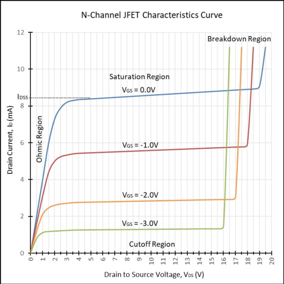
JFETs are unipolar devices that use an electric field to control current flow through a semiconductor channel. Each JFET consists of either an n-type or p-type channel bounded by two ohmic contacts: the source and drain. Current enters through the source and exits through the drain, while a reverse-biased pn-junction at the gate regulates the width of the conductive channel. As the reverse voltage increases, the depletion region expands inward, narrowing the channel and restricting current. When the gate voltage reaches a sufficiently negative value relative to the source (in an n-channel device), conduction effectively stops—a condition known as pinch-off. In comparison to MOSFETs, JFETs do not use an insulating oxide layer at the gate. Instead, their gate-channel interface is a physical junction, which simplifies the structure and makes them inherently depletion-mode devices.
This mode of operation gives JFETs several electrical advantages in IoT systems. First, they present extremely high input impedance, often in the teraohm range, which aids in interfacing with high-impedance sensors such as photodiodes, MEMS devices, and piezoelectric transducers. Second, JFETs draw virtually no gate current. Leakage levels typically fall within the picoampere to low nanoampere range, so that static power draw and offset errors are minimized.
Another strength is their low noise performance. JFETs generate minimal flicker noise (1/f noise). This is a boon for precision analog signal conditioning in low-frequency or broadband sensing applications. Finally, their operation is defined by voltage-controlled conductance. The drain current responds predictably to changes in gate-source voltage, allowing JFETs to serve as efficient, linear amplifiers in low-power analog signal paths.
Compared to MOSFETs, JFETs are better suited to analog signal integrity at low power levels. While MOSFETs can achieve even higher input impedance due to their insulated gate, this comes at the cost of higher gate leakage in some processes and greater susceptibility to electrostatic discharge. JFETs, by contrast, offer more robust protection and lower leakage but require a negative gate voltage, which may limit their compatibility with certain logic-level systems. Nevertheless, for analog front-end applications in energy-constrained environments, JFETs often deliver better overall performance than MOSFETs.
Power Efficiency and Low-Voltage Operation in IoT Devices
Power efficiency is often the most important design constraint in IoT devices. Where extended battery life and energy-conscious operation dictate component selection, power efficiency is top of mind.
JFETs are particularly well-suited to meet these demands because of their inherently low power consumption. Operating in depletion mode, they require little to no gate current and therefore draw negligible static power in both standby and active states. Their low bias current requirements further reduce energy usage.
In analog signal paths, JFETs offer highly efficient performance, as they provide linear gain characteristics even at low supply voltages and minimal quiescent currents. And, unlike bipolar devices that require significant base currents to remain active, JFETs can deliver useful transconductance with sub-microampere drain currents. This characteristic aligns well with the needs of energy-harvesting or long-duration IoT applications that hinge on every microampere.
For battery-powered systems, JFETs help minimize both static and dynamic power losses. Leakage current remains exceptionally low, which prevents battery drain during idle periods, while, at the same time, their analog linearity allows signal amplification with a fraction of the energy required by traditional amplifiers. As a result, JFET-based circuits can maintain high signal fidelity while extending operating life in constrained energy environments.
These benefits can be seen through a number of real-world applications. In piezoelectric sensing circuits, such as in vibration monitors or acoustic sensors, JFETs function as charge amplifiers. Their low input bias current prevents charge leakage and makes it easy to interface with high-impedance sources. Furthermore, in wireless sensor nodes, JFETs are often employed in ultra-low-power amplifier stages where environmental signals are weak and susceptible to noise. These stages rely on JFETs to amplify signals without introducing distortion or consuming excess power.
Noise Performance and Signal Integrity in IoT Sensors
Maintaining signal integrity in IoT sensor systems is often challenged by the presence of low-level analog signals and high-impedance interfaces. In these contexts, noise performance becomes a defining factor in determining system accuracy and reliability.
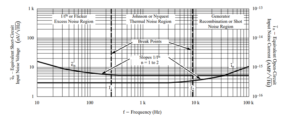
JFETs are well-regarded for their ability to support low-noise analog signal processing, especially in high-impedance circuits where traditional bipolar devices fall short. One of the advantages is their inherently low flicker noise. With low 1/f noise, JFETs are effective in low-frequency applications, such as bio signal monitoring and environmental sensing, where signal components lie in the sub-kilohertz range.
In addition to flicker noise suppression, JFETs also exhibit reduced thermal noise due to their channel geometry and unipolar carrier transport. Whereas BJTs involve both electron and hole conduction and introduce shot noise through base current flow, JFETs rely solely on majority carriers. This simplifies the noise profile and helps preserve weak signals in noise-sensitive systems.
These properties make JFETs a strong candidate for sensor front-ends with high source impedance. Electrochemical sensors such as pH meters and gas detectors often produce small current outputs that must be measured without introducing loading effects. Because JFETs present gate impedances in the teraohm range and draw only picoamperes of leakage current, they prevent charge drain and preserve the sensor’s output characteristics. Similarly, MEMS-based devices such as accelerometers and gyroscopes benefit from JFET-based amplification.
To further optimize noise performance, designers often turn to specific circuit design techniques. Selecting low-capacitance JFETs reduces parasitic coupling and improves high-frequency performance, which can help when dealing with broadband sensors or when the layout introduces long traces and stray capacitances. Another approach is the use of source degeneration resistors, which linearize the transconductance curve and increase noise rejection. This technique also stabilizes gain in variable environmental conditions, as can be encountered in field-deployed IoT nodes.
Temperature Stability and Environmental Reliability
Temperature and environmental reliability are central considerations for IoT devices deployed in industrial, automotive, and aerospace environments. These systems must operate consistently across wide temperature ranges, under varying humidity conditions, and sometimes in the presence of radiation. In these scenarios, JFETs offer distinct advantages over other transistor types.
One of the differentiators is gate leakage behavior. MOSFETs use an insulated gate formed by a thin oxide layer, which is susceptible to leakage current increases at elevated temperatures. As temperature rises, oxide insulation can degrade and cause significant variations in gate current that compromise analog precision and increase static power consumption. In contrast, JFETs rely on a reverse-biased pn-junction to control conduction. This junction remains stable across a broad temperature range, and the associated leakage current increases only marginally with temperature. As a result, JFETs exhibit far greater predictability and lower drift in high-temperature environments.
This thermal robustness is valuable in remote IoT devices that must remain operational without maintenance for years. For example, applications such as pipeline monitoring or engine diagnostics often face ambient conditions exceeding 85°C. JFETs maintain their performance in these environments without requiring additional compensation circuitry and thereby reduce system complexity and extend product lifetime.
Beyond temperature, JFETs also show resilience in radiation-prone environments. In aerospace and high-reliability industrial applications, exposure to ionizing radiation can induce charge buildup in a MOSFET’s gate oxide that causes threshold voltage shifts and functional failure. JFETs are inherently immune to this failure mode because they do not rely on an oxide gate. Radiation-hardened JFETs can tolerate total ionizing dose effects and displacement damage without significant performance degradation.
Moreover, JFETs demonstrate strong tolerance to electrostatic discharge (ESD) and voltage transients. The gate junction behaves like a diode, capable of safely clamping overvoltage conditions in many cases. This characteristic adds a layer of robustness to IoT front-end circuits exposed to frequent electrical disturbances, such as industrial motor systems or large-scale environmental sensing grids.
IoT Application Examples
Given the many benefits that JFETs offer IoT designers, there are naturally many different applications where the technology is being used today.
Wireless Sensor Nodes
In wireless sensor networks utilizing protocols like LoRa, Zigbee, or Bluetooth Low Energy (BLE), the RF front-end requires sensitive and power-efficient analog signal conditioning. JFETs improve front-end performance by reducing input-referred noise in the receiver chain and buffering weak signals without loading the preceding antenna or matching network. For example, in environmental monitoring stations deployed for wildfire detection, sensor nodes collect small analog signals from temperature or gas sensors and transmit the data wirelessly over long ranges. JFETs in the analog front-end of these sensor nodes help maintain signal integrity while allowing the entire node to operate from a small battery or solar energy harvester. Similarly, wildlife tracking tags using compact, energy-efficient RF circuits benefit from JFET-based amplifiers to reliably capture and transmit low-strength sensor data without sacrificing battery life.
Battery-Powered Medical Devices
In medical IoT devices, JFETs are used in analog circuits designed to detect and amplify extremely weak biosignals. In wearable monitors for ECG or EEG, signal levels can fall into the microvolt range, and any added noise or leakage current could obscure clinically relevant information. JFETs, with their ultra-low flicker noise and negligible input bias current, serve as the input stage to instrumentation amplifiers and help preserve signal fidelity. For example, a wearable EEG headset that records brain wave activity during sleep studies may integrate JFET-based front-ends to guarantee accurate signal capture over many hours without requiring recharging or recalibration.
Industrial IoT (IIoT)
Industrial IoT systems also leverage JFETs for vibration and acoustic monitoring in condition-based maintenance. In rotating machinery, piezoelectric sensors detect mechanical anomalies by generating charge in response to vibration. JFETs act as charge amplifiers or transimpedance amplifiers in these interfaces, converting weak sensor outputs into usable voltage signals while rejecting common-mode noise. Systems that monitor bearings, turbines, or motors in factories or remote infrastructure can run continuously for years by relying on the JFET’s stability and efficiency to avoid frequent maintenance or recalibration.
Future Trends and Design Tips
As IoT applications continue to push for smaller, smarter, and more energy-efficient designs, JFET technology is evolving to meet new demands.
Looking forward, advances in semiconductor processing are enabling the integration of complementary materials and device architectures, such as SiC-based JFETs with GaN HEMTs, into unified hybrid systems. While still emerging, hybrid transistor designs demonstrate how JFET-like structures can be tightly coupled with high-speed logic for efficient power switching and signal control. This progress suggests that JFET-on-CMOS or similar hybrid technologies could become a promising path for next-generation designs.
For IoT designers, JFETs remain a building block in high-impedance, low-noise circuits. Their stable leakage performance, low flicker noise, and minimal static power draw make them a great choice for sensor front-ends in always-on, energy-constrained environments. Designers should also consider hybrid JFET-MOSFET topologies, such as using a JFET input stage to drive a MOSFET-based output buffer, to balance analog precision with digital control and drive capability. One practical example is the use of a JFET differential pair feeding a CMOS op-amp core in wearable biosignal amplifiers. Such a design could combine low-noise acquisition with energy-efficient signal processing to empower battery-powered healthcare devices.
Conclusion
By combining the unique strengths of JFETs with modern integration strategies, designers can build the next generation of IoT systems that are low-power, high-performance, and ready for the demands of real-world deployment.