Semiconductor Manufacturing With Microdispensing Technology
Manufacturing semiconductors is made simpler and more cost-effective with the use of cutting-edge microdispensing technologies that can print on a range of substrates.

19 May, 2025. 3 minutes read
There are many uses for semiconductors. With their ability to process data, control electrical current, and power electronic devices, they are the building blocks of modern technology. This makes semiconductor fabrication a big business, and one in which any minor or major production gain must be treated like gold dust.
But what are these high-value materials exactly? In short, semiconductors are materials that conduct electricity to a certain degree, but not as well as a true conductor. Crucially, this conductivity can be controlled and modified by adding impurities in a process known as doping. This makes these materials incredibly useful for electronic applications. By controlling the conductivity of a material, engineers can turn it into an electronic switch, and this can be the basis for components like transistors, diodes, and integrated circuits.
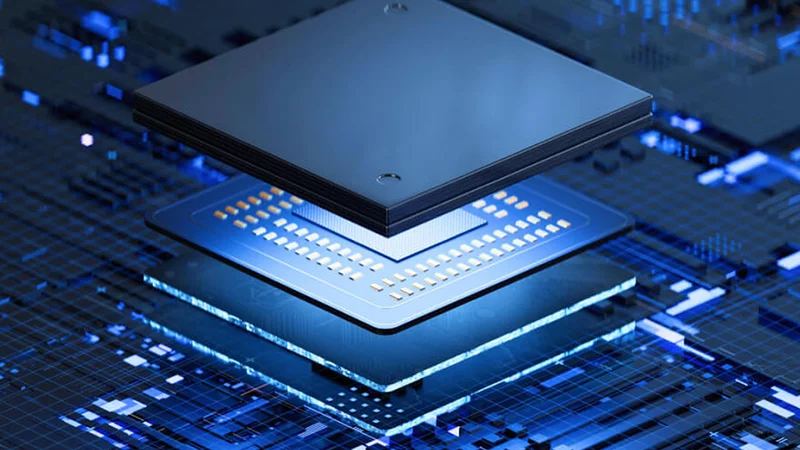
Manufacturing semiconductors generally involves a wafer manufacturing process, the introduction of circuit patterns via photolithography and etching, doping to modify the electrical properties of the semiconductor, and a variety of other sub-processes.[1] This article looks at how microdispensing can be used as a deposition technique to improve semiconductor manufacturing, adding new levels of precision with the application of nanoinks and nanopastes.
Key Challenges in Manufacturing Semiconductors
The semiconductor industry is critical to many aspects of modern life, with complex microchips now essential to the operation of public and private systems across the world. However, as the global chip shortage of the early 2020s proved, the semiconductor industry regularly faces challenges, from supply chain issues to skilled labor shortages.
Technical challenges are as common as logistical ones. As transistors become smaller, typical semiconductor packaging and interconnects may struggle to meet performance and power demands. However, one means of achieving better performance while minimizing power demands and footprint is to use a three-dimensional integrated circuit in which several interconnects are stacked vertically. But although the advantages of 3D ICs are significant, they present significant manufacturing challenges, heat management issues, and lower yields due to their complexity.
In fact, one of the biggest challenges in semiconductor manufacturing overall is production yield. Defects, faults, process variations, and design issues—caused by issues such as contamination, scratches, and pattern transfer between mask and wafer—can all lead to a reduction in yield, leading to fewer usable semiconductors from the batch.[2]
How Microdispensing Can Revolutionize Semiconductor Manufacturing
Some of the challenges associated with semiconductor manufacturing can be solved by using novel technologies that differ from established manufacturing techniques like photolithography and etching. For instance, XTPL’s Ultra Precise Dispensing (UPD) technology is a type of microdispensing that is ideal for fabricating ultra-precise conductive connections on semiconductor packaging and other components.
UPD, which can also be considered a type of direct ink writing, is ideal for manufacturing semiconductors for several reasons. First, its paste extrusion technology enables the additive deposition of a broad range of conductive and insulating materials with micrometric precision. The fine lines it produces encourage heat dissipation, reducing thermal issues in advanced 3D interconnects. Second, its deposition method allows for printing on a wide range of substrates, including silicon wafers and other fragile and topologically challenging surfaces. Another crucial benefit is its high suitability for defect repair, which can mitigate issues with production yield by correcting defective components.
XTPL’s technology can be used to make precise conductive connections, which are important for semiconductor components in devices like LED and OLED lighting. Depending on its application, it may be used as a substitute for an existing semiconductor manufacturing process or in addition to it (to correct defects, for example).
Current Applications and Future Possibilities
XTPL’s Ultra Precise Dispensing technology has been utilized by semiconductor manufacturers for several years now. In 2022, a Taiwanese company that builds manufacturing equipment for the semiconductor industry ordered an XTPL UPD module to be integrated into one of its manufacturing systems. That prototype manufacturing system, designed for the production of advanced semiconductor packaging, was then deployed by a large Taiwanese semiconductor manufacturer.
That successful use of a UPD module on the production line was just the start for XTPL in the semiconductor industry. In fact, this critical sector is one of XTPL’s main target markets, as the company’s UPD technology excels at creating 2D or 3D interconnects on complex topographies and heterogeneous substrates in advanced integrated circuits.
With its ability to be integrated into existing semiconductor manufacturing equipment on the production line, the XTPL UPD module has the potential to greatly increase semiconductor complexity, facilitate more efficient testing, mitigate thermal challenges, and increase production yield as the industry transitions into 2nm process era in the second half of 2025.
Resources
[1] Chao TS. Introduction to semiconductor manufacturing technology. New Jersey: Prentice Hall; 2000.
[2] Semiconductor Industry Association. International technology roadmap for semiconductors. 2009.