Multilayer PCBs and the Cutting-Edge of Circuit Board Repair
Multilayer PCBs are at the forefront of printed electronics today but bring with them some challenges related to testing and repair.

30 May, 2025. 4 minutes read
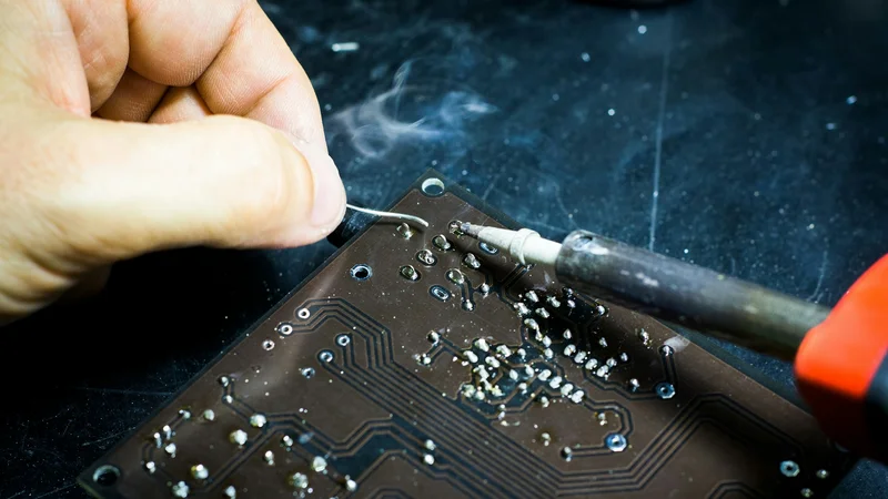
Photo by Blaz Erzetic on Unsplash
Multilayer printed circuit boards (PCBs) represent a growing proportion of PCBs made today, with the growth driven in large part by the increased demand for miniaturized electronics. It makes perfect sense: after all, smaller electronic devices necessitate the compaction of circuits without decreasing functionality. In this article, we’ll be looking more specifically at testing and repair techniques for multilayer PCBs and the challenges that this type of circuit brings up. We’ll also be talking about technologies at the forefront of PCB repair, including XTPL’s direct writing platform.
Understanding Multilayer PCBs
Before diving into repair methods for multilayer PCBs, it is first important to understand the role of this type of circuit in the broader electronics industry. Generally speaking, there are different types of printed circuit boards, including single-sided PCBs, double-layer PCBs, and multilayer PCBs. The latter are the most complex and typically have the greatest functionality. In the simplest terms, this is because combining multiple layers into a single PCB makes it possible to increase the amount of circuitry without significantly increasing the board’s footprint.
While any PCB with at least three layers is considered a multilayer PCB, it is technically possible to have hundreds of layers in a single PCB. In a smartphone, most PCBs have around 10 layers.[1] Unlike single-layer PCBs, which consist of a conductive layer on a substrate, multilayer PCBs sandwich conductive layers (typically copper foils) and insulating layers (prepregs and core) above and below a rigid substrate.
There are several benefits to integrating multilayer PCBs in electronic devices, including greater circuit density, which allows for greater functionality and performance while economizing on size. Multilayer PCBs also tend to be higher in quality since they require more in-depth planning at the design stage than simpler PCBs.
Despite these benefits, however, multilayer PCBs do bring with them an added level of complexity, not only in terms of production methods but also when it comes to repair. This complexity is driven by a couple of factors. For one, identifying where a fault exists in the multilayer PCB is far more challenging than with a single-sided PCB, since a defect can be located on one of the board’s inner layers. When the fault is found, it then requires extreme precision to repair it without damaging or compromising the rest of the board. Unfortunately, these challenges have often meant that whenever a multilayer PCB isn’t functioning properly, it has to be completely replaced.
Diagnostic Techniques for Multilayer PCBs
Fortunately, advanced technologies and manufacturing methods are unlocking more effective diagnosing and repair of defective multilayer PCBs. Let’s take a look at some of the techniques that are making a difference.
In order to identify a defect in a multilayer PCB, electronics manufacturers and repair shops can use a variety of diagnostic tools, such as a multimeter, which can measure the current of the PCB at different points to find an open circuit. In-circuit testing (ICT) is another commonly used method, which positions probes at specific points of the PCB to measure resistance and other factors. Both of these quality control tests are non-destructive and can thus be helpful for finding a defective circuit, but may be limited when it comes to finding the exact location of a broken or weak trace.
For this, there are more advanced non-destructive processes, like X-ray scanning or automated optical inspection (AOI). X-ray technology can capture images of the internal structure of a multilayer PCB and reveal specific defects. AOI, for its part, uses specialized high-res cameras and advanced software to scan multilayer circuits, comparing the final product to the original Gerber file to identify any discrepancies. With AOI, it is key that the layers of a multi-layer PCB are scanned before final assembly and lamination.
Repairing Multilayer PCBs
Unfortunately, the repair of multilayer printed circuit boards remains a big challenge in the electronics industry. It’s easy to understand why: if there is any defect or damage to one of the inner laminated layers of a PCB, it is very difficult (and in some cases impossible) to get inside to repair it without damaging or compromising another element of the board.
There are techniques like microdilling that can give repair professionals access to a defective trace inside a multilayer PCB. In most cases where this is possible, a defective trace or via would have to be rerouted using a conductive trace or wire. Generally, delaminating a multilayer PCB is not recommended since it is both time and cost consuming.
There are also other PCB board repair techniques that can be implemented for multilayer PCBs, particularly when a defect is located on the board’s surface. For example, direct writing processes like XTPL’s Ultra-Precise Dispensing (UPD) technology can repair open defects in PCBs with a high degree of efficiency and precision. More specifically, UPD uses a pressure-based dispenser to selectively deposit conductive nanoinks or nanopastes onto a substrate. Notably, the technology is capable of dispensing traces and lines with a resolution of 1 µm, making it suitable for miniaturized electronic circuits.
When it comes to PCB repair, XTPL’s UPD technology can fill in broken or too-thin traces with a conductive ink, like Ag Nanoink CL34, a conductive silver ink with up to 50% bulk silver conductivity. The company’s silver Nanopaste CL85, one of its flagship products, offers a higher viscosity that makes it possible to apply the material to vertical surfaces and 3D topographies with a high level of accuracy.
XTPL, at the Forefront of PCB Repair
Ultimately, dispensing processes like XTPL’s UPD are suitable for circuit board testing and repair, particularly when it comes to single-sided and double-layer PCBs. But they can also be employed to repair the surfaces of multilayer PCBs or inner circuits before they are laminated, helping electronics manufacturers to overcome some of the challenges of repairing multilayer PCBs.
Resources
[1] PCB Design Requirement for Smartphones [Internet]. PCB Cart, 2025. https://www.pcbcart.com/article/content/design-pcbs-for-smart-phones.html