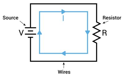
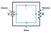
Protect sensitive electronics by understanding the current limiting resistor, learning how to calculate appropriate values, and applying them in LEDs, transistors, microcontroller inputs and other circuits.
This guide explains how potentiometer pins interact with mechanical rotation, resistive tracks, and load conditions across various circuit configurations. It provides clarity for both low-power electronic designs and high-precision embedded systems.
This technical article explains the theory behind potentiometer schematics. It shows how to implement mechanical and digital potentiometers in practical circuits, tailored for engineers, and students.
Engineering teams can achieve AI-ready design data with five-level maturity model by Keysight. The unified, traceable data accelerates design cycles, boosts IP reuse, and reduces costly re-spins.
Focused laser-like light that covers a wide range of frequencies is highly desirable for many scientific studies and for many applications, for instance quality control of manufacturing semiconductor electronic chips.
Scientists at ITMO have come up with a new way to protect microelectronics devices from counterfeit. The new technology is based on gold and silicon nanoparticles with unique optical properties that make it possible to create unclonable functions with a record information density.
An international team of scientists was first to demonstrate that halide perovskites can serve as a base for nonlinear on-chip optical components. As an example, they can be used to build ultrafast optical chips and transistors, and, potentially, other integrated optical systems.
PCB etching is a chemical process that removes copper to form circuits. This guide covers fast etchants, FeCl₃ reactions, AI-driven optimization, aerospace standards, and sustainable methods for high-density PCBs in 5G and medical applications.
The EIT series encompasses a range of technologies, with each installment focusing on specific engineering challenges and how sensor integration, power optimization, and design-for-sustainability principles are reimagining sustainable electronics from the ground up.
Learn how to wire a potentiometer in various configurations (voltage divider, rheostat, sensor) with this in-depth guide. We cover various potentiometer types, provide step-by-step wiring instructions, offer circuit design tips, highlight common mistakes, and include real-world examples.
Scientists at ITMO have come up with a new way to protect microelectronics devices from counterfeit. The new technology is based on gold and silicon nanoparticles with unique optical properties that make it possible to create unclonable functions with a record information density.
Polymer glass transition temperature (Tg) refers to the temperature at which an amorphous polymer transitions from a glassy, rigid state to a rubbery, flexible state. Understanding the polymer glass transition temperature is crucial for various industries, including engineering and manufacturing.
aster KCL circuit analysis with our comprehensive engineering guide covering nodal analysis, modern simulation tools, and industry applications. Learn advanced techniques used by leading engineers. Start optimizing your circuit designs today.
Azoteq's IQS39x family combines capacitive sensing and haptic feedback in a single compact IC, enabling more responsive, intuitive, and reliable user interfaces for next-gen consumer, industrial, and wearable devices.
Researchers at ETH Zurich and Empa have developed a new image sensor made of perovskite. This semiconductor material enables better colour reproduction and fewer image artefacts with less light. Perovskite sensors are also particularly well suited for machine vision.
Plasma Science and Fusion Center researchers created a superconducting circuit that could one day replace semiconductor components in quantum and high-performance computing systems.
Discover how Dry Phase Patterning (DPP) showcased a 99 percent reduction both in carbon footprint and electricity used compared to conventional wet etching.