How Does SPI Work? A Comprehensive Guide for Digital and Hardware Engineers
This article answers the practical question: how does SPI work, detailing the theory behind the bus, the role of each signal, timing modes, architectures and topologies, and practical design considerations.

06 Oct, 2025. 14 minutes read
Serial Peripheral Interface (SPI)
Introduction
Modern embedded systems rely on reliable communication between controllers and peripherals. Engineers often ask a fundamental question: how does SPI work? Serial Peripheral Interface (SPI) has become a cornerstone of digital communication due to its simplicity, speed, and scalability. Understanding how SPI works is crucial for designing circuits that effectively handle sensors, displays, memory modules, and communication chips.
SPI enables full-duplex data exchange with minimal wiring, making it attractive for low-latency and high-performance designs. To answer, how does SPI work, one must analyze the four essential signals: MISO, MOSI, SCK, and SS, and how timing relationships define data integrity. These details separate successful implementations from unreliable prototypes.
This guide explores theory, implementation, and engineering practices, helping digital and hardware professionals answer the practical question: how does SPI work in real-world applications while ensuring efficient communication.
Fundamentals of SPI Communication
Synchronous Serial Communication
The defining feature of the Serial Peripheral Interface (SPI) is its synchronous nature. In synchronous serial communication, all data transfers are aligned with a shared clock signal, ensuring that the transmitter and receiver sample bits at precisely the same time. This contrasts with asynchronous protocols like UART, where synchronization depends on start and stop bits combined with a predefined baud rate. Such framing introduces overhead and limits maximum throughput.
By sharing a dedicated serial clock (SCLK) generated by the microcontroller (master), SPI communication achieves much higher data transfer rates, often reaching tens of megahertz. The absence of framing overhead makes it well-suited for short-distance, high-speed interconnects within embedded systems.
Signals and Pin Functions
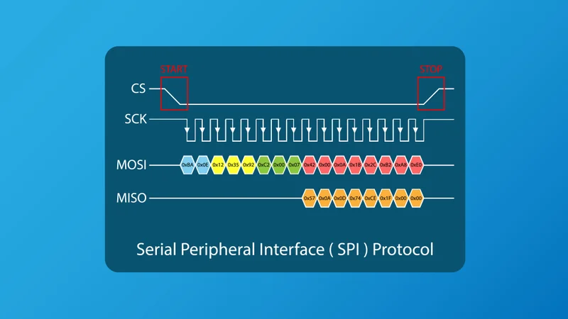
Standard SPI implementations use four signals: a clock, a chip‑select line, and two unidirectional data lines. The table below summarises these signals as follows:
| Signal | Common Names | Purpose |
| SCLK | Serial Clock | Generated by the Controller to Synchronise Data Transfer |
| PICO/MOSI | Peripheral In Controller Out (Master Out Slave In) | Carries Data from the Controller to the Peripheral |
| POCI/MISO | Peripheral Out Controller In (Master In Slave Out) | Carries Data from the Peripheral to the Controller |
| CS/SSN | Chip Select / Slave Select (Active‑Low) | Selects the Target Peripheral; Asserted low to Initiate a Transaction |
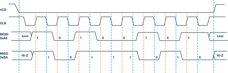
Once the controller asserts CS low and toggles SCLK, it shifts data on MOSI while simultaneously receiving data on MISO. Because data lines are unidirectional and independent, SPI naturally supports full-duplex communication. This capability distinguishes it from I²C, which relies on a single bi-directional line, resulting in half-duplex operation.
Different manufacturers may use alternative naming conventions, such as PICO/POCI (Peripheral In/Out), to avoid the master/slave terminology. Regardless of naming, the function of each signal remains identical across implementations.
Clock Polarity, Phase, and Modes
The flexibility of SPI comes from its configurable timing. Two parameters, Clock Polarity (CPOL) and Clock Phase (CPHA), determine the precise relationship between data and clock transitions [1]:
CPOL: Defines whether the idle state of SCLK is logic low (0) or logic high (1)
CPHA: Defines whether data is sampled on the first or second clock edge
The combination of CPOL and CPHA produces four distinct SPI modes:
| Mode | CPOL | CPHA | Description |
| 0 | 0 | 0 | Clock Idles Low; Data Sampled on Rising Edge and Shifted on Falling Edge |
| 1 | 0 | 1 | Clock Idles Low; Data Sampled on Falling Edge and Shifted on Rising Edge |
| 2 | 1 | 0 | Clock Idles High; Data Sampled on Falling Edge and Shifted on Rising Edge |
| 3 | 1 | 1 | Clock Idles High; Data Sampled on Rising Edge and Shifted on Falling Edge |
The datasheet of each device specifies its required CPOL/CPHA combination. For example, the analog devices application note states that the SPI interface allows the user to choose the rising or falling edge of the clock to sample and/or shift data. In practice, mode 0 (CPOL = 0, CPHA = 0) is common for memory devices, while sensors may require mode 3.
Data Order and Word Length
Two further parameters affect SPI transfers: bit order and frame length.
Bit Order: Devices may shift out the most significant bit (MSB) first or the least significant bit (LSB) first. This is not standardized in the SPI protocol, so designers must confirm the required order in the datasheet. Microcontroller frameworks, such as setBitOrder() of Arduino, let developers select the appropriate setting. [2]
Word Length: While 8-bit transfers are most common, many peripherals support 16-bit, 24-bit, or 32-bit frames. Some devices, such as specialized converters or EEPROMs, may require fixed word lengths. The controller must generate the correct number of clock pulses while keeping CS low throughout the transaction.
Correctly setting data order and word length is essential for reliable SPI communication. It is better to consult the device datasheet and ensure the controller generates the right number of clock pulses per transaction.
Full-Duplex Operation
One key advantage of SPI over other communication protocols is true full-duplex operation. While the controller shifts out new command data on MOSI, the peripheral simultaneously shifts out previous data on MISO. This enables efficient real-time data transfer, for example:
Requesting a new sensor measurement while retrieving the last conversion result.
Writing a memory address while reading back stored contents in the same clock cycle.
This feature boosts throughput significantly compared to half-duplex buses like I²C. However, system designers must ensure proper timing so that returned data bits are valid during the corresponding clock edges.
Recommended Reading: I2C vs SPI: A Comprehensive Comparison and Analysis
SPI Bus Architecture and Topologies
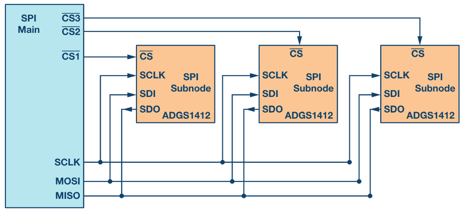
Understanding how SPI works requires examining the different ways devices can be connected. The architecture of SPI is simple: there is always one controller generating the clock and at least one peripheral. However, multiple topologies exist, each optimised for specific use cases. The figure below illustrates a typical SPI bus connecting one controller to two peripherals using separate chip‑select lines.
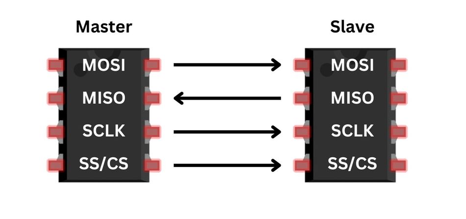
The controller communicates with two peripherals via separate CS lines. The clock (SCLK) and PICO/MOSI lines carry data from the controller, while POCI/MISO lines return data. Each peripheral has its own chip‑select line (CS1, CS2) to avoid bus contention.
Single Controller, Single Peripheral
The most fundamental setup is a single-master, single-slave connection. The four signal lines: SCLK, MOSI, MISO, and CS form the entire link. This topology is ideal when a microcontroller communicates with one memory chip, EEPROM, or sensor module. Because only one peripheral exists, there is no risk of bus contention, and configuration is straightforward. Many datasheets assume this topology as a baseline when describing device timing requirements.
Multiple Peripherals with Independent Chip-Select Lines
When multiple SPI devices share the MOSI, MISO, and clock lines, the controller assigns each a dedicated chip select pin. To communicate with a specific peripheral, the controller pulls the CS line of the device low while keeping all other lines high.
This method guarantees deterministic data transmission because only one peripheral drives the MISO line at a time. However, scalability is limited. If dozens of peripherals are needed, dedicating one GPIO pin per device quickly exhausts the controller’s I/O. Designers often use a decoder or multiplexer (e.g., 74HC238) to expand the number of selectable devices without consuming excessive pins.
Daisy-Chain Configuration
Some peripherals support a daisy-chain topology, where the MISO of one device connects directly to the MOSI of the next. All devices share a single chip select. The chain behaves like an extended shift register: each clock cycle shifts data further down the chain.
Advantage: Only one CS pin is required, greatly simplifying pin assignments.
Limitation: The controller must clock enough data bits to propagate instructions through all devices, which introduces latency for devices deeper in the chain.
This architecture is common in output-only systems such as LED driver ICs or shift registers, where the return path from peripherals is not critical.
3-Wire and Multi-I/O Variants
While four wires are typical, some systems use fewer. A 3‑wire SPI merges the PICO and POCI lines into a single bi‑directional data line called DIO. The TI application note states that the 3‑wire configuration reduces the number of wires to three: SCLK, CS, and DIO. [3] However, this sacrifices true full‑duplex operation because reading and writing cannot occur simultaneously. Some FPGAs and microcontrollers support this mode for space‑constrained designs.
SPI has evolved further into multi‑I/O interfaces such as Dual SPI, Quad SPI (QSPI), and Octal SPI. These expand the number of data lines to two, four, or eight, enabling much higher data transfer rates without raising the clock frequency. For instance, serial flash memory devices can achieve a throughput of over 50 MB/s using QSPI.
When using these variants, engineers must ensure:
The microcontroller or controller supports the desired mode.
The datasheet specifies instruction sets for multi-I/O transactions.
The signal integrity is maintained at higher switching speeds, particularly when routing multiple parallel lines on a PCB.
Recommended Reading: UART vs SPI: A Comprehensive Comparison for Embedded Systems
Advantages and Limitations of SPI
Speed and Performance
One of the most substantial advantages of the SPI protocol is raw speed. Because the serial peripheral interface has minimal overhead and no addressing frames, the bus can sustain very high data transfer rates.
Below is the detail:
Throughput: Many microcontrollers (e.g., STM32, TI C2000) can drive SPI at 50 MHz or more, while FPGAs may exceed 100 MHz.
Comparison: By contrast, the original I²C standard was designed for 100 kHz. Even its high-speed mode tops out at 5 MHz.
Applications: High frequencies enable rapid sensor sampling, low-latency data transmission in networking modules, and faster read/write cycles in memory chips or EEPROMs.
Because SPI does not enforce a maximum clock frequency, performance is limited primarily by signal integrity, device specifications, and PCB layout.
Flexibility and Simplicity
The SPI bus offers flexibility in both timing and configuration:
Separate MISO and MOSI lines allow true full-duplex communication, unlike I²C’s single bidirectional line.
Designers can adjust clock polarity (CPOL) and clock phase (CPHA), supporting four operating modes.
Devices may use different word lengths (8, 16, 24, or 32 bits per frame).
SPI can be implemented either via dedicated hardware or through bit-banging on general-purpose I/O pins.
Because there is no strict governing standard, manufacturers often tailor the SPI interface to device-specific requirements. This flexibility improves adaptability, but it also increases the burden on engineers to verify timing through the datasheet.
Versatile Applications
SPI is used in virtually every embedded domain requiring short-distance, high-speed communication. The examples include:
Memory Devices: Flash (NOR, NAND), SD cards, serial EEPROMs.
Sensors and Converters: Temperature sensors, ADCs, DACs.
Display and User Interfaces: TFT/LCD controllers, touch-screen drivers.
Industrial Modules: Digital potentiometers, motor controllers, shift registers.
Communication Modules: RF transceivers, audio codecs, real-time clocks, and Wi-Fi chipsets.
Its ability to handle full-duplex data transfer with low latency makes SPI especially valuable in real-time embedded systems.
Limitations and Design Trade-offs
Despite its strengths, SPI has several constraints:
- Wiring Complexity – At least four signal lines are required, plus a chip select for each peripheral. Systems with many devices quickly consume microcontroller I/O pins.
- Controller Driven Model – Only the master device initiates transactions; slave devices cannot request service or send data autonomously.
- Scalability Challenges – Each new slave device usually needs its own CS line. While Daisy-chain topologies reduce pin count, they add latency and complexity.
- Short-Distance Limitation – High-speed signals degrade quickly over long traces or cables. Beyond a few feet, designers must lower the clock frequency or use differential drivers.
- Non-Standardization – Unlike I²C, SPI lacks a formal standard. Variations in CPOL, CPHA, data order, and timing between vendors require careful datasheet checks.
In addition to these points, the lack of an official standard means that timing and bit ordering vary between devices. Engineers must carefully read datasheets and configure the SPI peripheral accordingly to avoid miscommunication.
Comparison with Other Protocols
It is often helpful to compare SPI with other common serial interfaces. The table below highlights how SPI, I²C, and UART differ:
| Feature | SPI | I²C | UART |
| Communication Type | Synchronous | Synchronous | Asynchronous |
| Data Transfer Mode | Full‑Duplex | Half‑Duplex | Full‑Duplex |
| Clock Signal | Yes | Yes | No |
| Addressing | CS Line | Address Frame | Not Applicable |
| Typical Speed | High | Medium | Low |
This table illustrates that while SPI offers the highest throughput, I²C excels in reducing wiring complexity (two wires), and UART is suited for long‑distance communication because it does not require a shared clock.
Recommended Reading: I2C vs SPI vs UART: A Comprehensive Comparison
Practical Implementation and Design Considerations
Configuring SPI in Microcontrollers
Most modern microcontrollers provide a hardware SPI peripheral.
The typical steps to initialise SPI are as follows:
Pin Configuration – Assign MOSI, MISO, SCLK, and chip select (CS) to their alternate functions. Some controllers allow flexible mapping, while others use fixed pins.
Bit Order Selection – Determine whether the device expects MSB-first or LSB-first transmission. It is better to verify through the device datasheet.
Clock Polarity and Phase – Select the correct CPOL/CPHA combination. A mismatch leads to corrupted data transmission. If multiple slave devices require different modes, reconfigure the interface before each transaction.
Clock Frequency – Match the clock speed of the controller to the specifications of the peripheral. Some sensors operate reliably at only a few MHz, whereas flash memory chips may support 50 MHz or more. Exceeding device limits risks communication errors.
Chip Select Management – Each transaction begins when CS is asserted low and ends when it returns high. Certain microcontrollers can toggle CS automatically, while others require manual control.
Proper SPI configuration ensures stable and efficient communication between the controller and peripherals. The careful attention to pins, timing, and device limits prevents errors and guarantees reliable system performance.
Selecting SPI Mode and Clock Parameters
Reliable communication depends on the proper selection of mode and frequency:
CPOL/CPHA settings must match the requirements listed in the datasheet of the peripheral.
Clock frequency should consider not only the maximum of the device but also system factors such as supply voltage, PCB layout, and required noise margins.
If multiple SPI devices are connected, dynamic reconfiguration of clock polarity, phase, and frequency may be necessary between transactions.
Aligning CPOL/CPHA and frequency with device specifications ensures accuracy, while careful reconfiguration across peripherals maintains system reliability.
Signal Integrity, Termination, and Board Layout
High‑speed digital signals are prone to reflections and interference. To ensure reliable communication:
Keep Traces Short and Matched: Run the PICO, POCI, and SCLK lines parallel and close together to minimise skew. Avoid long stubs or sharp turns.
Use Series Termination: Place small resistors (~30–50 Ω) near the driver to reduce ringing and overshoot on the clock and data lines.
Maintain Proper Grounding: Provide a continuous ground reference and use ground pins adjacent to SPI signals when possible.
Reduce Clock Speed for Long Distances: Lower the clock speed and use specialized driver chips when signals need to travel more than a few feet.
Maintaining signal integrity is critical for high-speed SPI communication. Careful routing, grounding, and termination practices reduce noise and reflections, ensuring stable data transfer across different board layouts and operating conditions.
Debugging and Analysing SPI Traffic
When SPI communication fails, visibility into signal behavior is essential:
Logic Analysers – Capture MOSI, MISO, CS, and SCLK simultaneously. Many tools decode SPI signals into readable hexadecimal data, indicating whether the bytes align with expected transactions.
Protocol Analysers – Instruments such as Total Phase’s Beagle can track SPI traffic up to 24 MHz with nanosecond-level resolution, useful for verifying timing against specifications.
Oscilloscopes with Serial Decode – Allow inspection of both analog signal quality and decoded data bits, confirming correct clock edges, polarity, and identifying jitter, skew, or noise.
Effective debugging tools give engineers deep insight into SPI signals and timing behavior. Using logic analysers, protocol analysers, or oscilloscopes ensures precise validation, helping detect errors early and maintain reliable data transmission.
Recommended Reading: ESP32 Pinout: A Comprehensive Guide for Engineers
Advanced SPI: Multi‑line and High‑Throughput Variants
Today, modern systems demand higher bandwidth for external storage and display interfaces, and designers increasingly turn to multi-I/O SPI extensions. [4]
These advanced implementations build on the classic serial peripheral interface (SPI) by widening the data lines, enabling higher throughput without excessively raising the clock frequency.
Dual, Quad, and Octal SPI
Dual SPI uses two data lines, allowing data to be clocked in or out on both simultaneously. This nearly doubles the effective data transfer rate compared to standard single-line operation.
Quad SPI (QSPI) expands to four data lines, commonly used in serial flash memories and supported by many microcontrollers such as the ESP32 and STM32H7. QSPI enables XIP (Execute In Place), where code runs directly from external flash instead of being copied into SRAM, saving valuable internal memory resources.
Octal SPI extends the same concept to eight data lines, providing throughput suitable for advanced applications such as high-resolution graphics, machine learning accelerators, and real-time automotive systems.
While these modes reduce latency and boost bandwidth, they introduce greater complexity in board layout and require precise signal integrity measures due to multiple high-speed data transitions occurring simultaneously.
QSPI DDR (Double Data Rate)
QSPI DDR is an additional performance extension, where data transitions occur on both the rising and falling clock edges. This effectively doubles throughput without increasing clock frequency, making it ideal where signal integrity becomes a bottleneck.
However, DDR introduces stricter timing requirements:
Setup and hold times must be tightly controlled
Clock skew across multiple data lines can cause bit misalignment
Careful PCB routing with length-matched traces and controlled impedance becomes mandatory
Designers often rely on FPGA-based controllers or advanced SoCs with built-in calibration logic to reliably operate in DDR mode.
Design and System Considerations
When implementing multi-line SPI, engineers must ensure:
Controller and Memory Compatibility – Both must support the same command set and multi-I/O instructions.
Clock Frequency Balance – Even with more data lines, exceeding the device’s maximum rated clock frequency risks errors.
Board Layout – Each additional line increases routing density. Use solid grounding, controlled impedance, and matched trace lengths.
Power Consumption – Wider buses and faster edges increase switching currents, requiring robust power distribution networks.
Firmware Configuration – Initialization sequences often differ from standard SPI and may require custom drivers or HAL support.
For very high-end designs, such as FPGAs, GPUs, or data center modules, even advanced SPI cannot meet the required bandwidths. Protocols like Serial RapidIO, HyperBus, or PCIe are chosen instead, achieving gigabit-per-second data transfer rates and offering additional features like addressing, error correction, and advanced flow control.
SPI in Modern Embedded Systems and Market Trends
Market Growth and Statistics
The popularity of SPI is underscored by market data!
The global SPI market is projected to reach USD 8.2 billion by 2033 with a compound annual growth rate (CAGR) of around 7.2%.
The Serial (SPI) NOR Flash segment alone was also at USD 4.5 billion in 2024, with forecasts estimating growth to about USD 9.2 billion by 2033.
The SPI flash market overall (across EEPROM, 3D NAND, etc.) rose from about USD 1.06 billion in 2024 to USD 1.11 billion in 2025, and is expected to grow to ~USD 1.45 billion by 2030 under current projections.
The surge in connected devices further fuels adoption. The number of IoT devices worldwide is projected to surpass 29 billion by 2030, nearly tripling the 2020 quota of 9.7 billion. Each IoT node often includes one or more SPI peripherals (sensors, memory, radios), highlighting how integral SPI has become to the IoT ecosystem.
Typical Applications and Case Studies
Some prominent applications of SPI include:
Sensors and Data Acquisition: Many MEMS sensors (accelerometers, gyroscopes, temperature sensors) use SPI because it supports rapid data sampling with minimal latency. For example, Total Phase lists temperature sensors and touch‑screen controllers among SPI‑driven devices.
Memory Devices: Serial NOR and NAND flash memories rely on SPI or QSPI for read/write operations. The TXE8116/24 example from TI uses a 24‑bit SPI frame with MSB‑first transmission. QSPI is common in microcontrollers that execute code directly from external flash.
Audio Codecs and Display Drivers: High‑resolution audio converters and LCD/LED drivers use SPI for streaming data because of its throughput and predictable timing.
Communication Modules: RF transceivers (e.g., Bluetooth or Wi‑Fi modules) often expose an SPI interface to configure registers and transfer packets.
Automation and Motor Control: In industrial control, SPI connects digital potentiometers, ADCs/DACs, and motor drivers to central controllers. Daisy‑chain configurations allow multiple devices to be cascaded with minimal wiring.
These diverse applications highlight the adaptability of SPI across industries. From high-speed memory access to precise motor control, the protocol remains a cornerstone of embedded design, ensuring reliable, low-latency communication in modern electronic systems.
Recommended Reading: SPI Protocol: Revolutionizing Data Communication in Embedded Systems
Conclusion
The Serial Peripheral Interface (SPI) remains a cornerstone of modern embedded systems. SPI is a synchronous, full‑duplex bus using separate transmit and receive lines, a shared clock, and chip‑select signals. Its simplicity and high throughput make it ideal for sensors, memory devices, communication modules, and industrial automation. Designers must carefully manage CPOL/CPHA, wiring complexity, and signal integrity to ensure reliable operation. Looking forward, advanced variants like Dual, Quad, and Octal SPI will drive higher performance, enabling execute-in-place flash and high-resolution displays. With IoT devices surpassing tens of billions, mastering SPI remains essential for digital and hardware engineers worldwide.
Frequently Asked Questions
Q1. What does full‑duplex mean in SPI?
A. Full-duplex means data is transmitted and received simultaneously over dedicated lines. Unlike I²C, SPI allows the controller to send commands while the specific slave device responds on the MISO line.
Q2. How many devices can I connect to an SPI bus?
A. There is no strict limit, but each integrated circuit generally requires its own SS line. For larger systems, use multiplexers or daisy-chain topologies, though daisy-chains increase latency due to serial shifting.
Q3. Can SPI be used over long distances?
A. SPI is intended for short-distance communication, usually on the same PCB. Signal quality degrades with length. Designers reduce clock speed or add drivers, but beyond meters, consider alternatives like RS-485 or CAN.
Q4. What are the advantages of SPI over I²C?
A. SPI provides higher throughput, full-duplex communication, and flexible word sizes. It simplifies signalling since no addressing frames are required. I²C, however, uses fewer wires and supports multiple masters, making it attractive for pin-limited applications.
Q5. Do all SPI devices use the same pin names?
A. No. To avoid master/slave terminology, some manufacturers use PICO/POCI for Peripheral In/Out and CS instead of SSN. Others still use MOSI/MISO/SS. It is better to see the tutorial or refer to the manufacturer’s documentation to map signal names correctly.
References
[1] Analog Devices. Introduction to SPI Interface [Cited 2025 September 25] Available at: Link
[2] ResearchGate. Integrated Development Environment "IDE" For Arduino [Cited 2025 September 25] Available at: Link
[3] Analog Devices. SPI/I2C Bus Lines Control Multiple Peripherals [Cited 2025 September 25] Available at: Link
[4] Wevolver. SPI Protocol: Revolutionizing Data Communication in Embedded Systems [Cited 2025 September 25] Available at: Link
in this article
1. Introduction2. Fundamentals of SPI Communication3. SPI Bus Architecture and Topologies4. Advantages and Limitations of SPI5. Practical Implementation and Design Considerations6. Advanced SPI: Multi‑line and High‑Throughput Variants7. SPI in Modern Embedded Systems and Market Trends8. Conclusion9. Frequently Asked Questions10. References